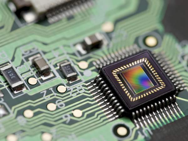
Photonics Solutions for Semiconductor Manufacturing


Rising Demand for Electronics Fuels Semiconductor Equipment Growth
Ever since the first solid state devices were invented, there has been a fast-growing demand for electronics in all aspects of our lives. We don’t think this is going to stop any time soon. Some of the areas that are driving the current and future demand for electronics: personal electronic devices, artificial intelligence, higher-tech automobiles, the rollout of 5G networks, more and larger data centers, and the Internet of Things. What this means for the semiconductor wafer fab equipment market is that within a few years its worldwide revenues could surpass $100 billion.
One of the challenges with electronic devices from the beginning was to make them not only smaller but also more powerful. There was a time when a simple computer took up much of an entire room, but today that little smart watch on your wrist is far more powerful and useful than much larger sized computers of 40 and 50 years ago. Exponential growth in the number of transistors per processor has enabled this to occur. To keep up with the increasing technological demand, new designs and manufacturing processes for semiconductors are going to be needed.
MKS Solutions and Products
MKS is more than just a provider of great products for semiconductor manufacturing. We are your partner who can provide the solutions you need to help meet the current and future semiconductor manufacturing challenges.
| Challenges in Semiconductor Manufacturing | MKS Solutions |
|---|---|
| Maximizing throughput | High speed, high acceleration motorized positioners High power lasers with programmable pulse shapes High power/high fluence optics |
| Maximizing yield | High accuracy, high repeatability motorized positioners Optics for manipulation of DUV and EUV light |
| Reducing size / increasing transistor density | DUV and EUV optical components and/or assemblies |
| Building the Optimal System | Applications engineering expertise & full range of products |
The first challenge that often comes to mind is maximizing throughput. We’re talking hundreds of billions to a trillion or so of integrated circuits produced every year, so manufacturing has to be both fast and plentiful. MKS’ motorized positioners, specifically our air-bearing, linear motor platforms, provide the high speed needed for applications such as inspection and lithography. And as electronic devices become smaller and smaller, we believe that more of the semiconductor manufacturing processes will need to become laser-based, and MKS offers lasers, including high power lasers with pulse control, that can be used for inspection, dicing, marking, low-k grooving and package cutting and drilling. And to work with high power lasers for optimal results, MKS can also provide high power/high fluence optics.
Along with maximizing throughput, another challenge is maximizing yield. Once again, our motorized positioners offer very high accuracy and repeatability to ensure the best results over and over again.
A trend we’re seeing with the desire to increase transistor density while continually reducing the size of electronic devices is more use of DUV and EUV light throughout the semiconductor manufacturing process. MKS can provide the optics and components necessary to manipulate and manage these wavelengths, which will also lead to higher yield.
Finally, the optimal system has to be built. This means choosing the appropriate components based on performance, form factor, cost and other considerations, and making sure everything works well together. Not only does MKS offer a full range of products in all product categories, but we also have a dedicated team of applications engineers that can help select the appropriate products and also integrate and optimize the system for your needs. They’ll provide a crucial link between your technical staff and MKS’ engineers.

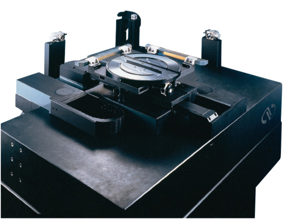
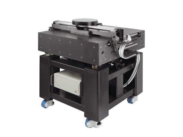
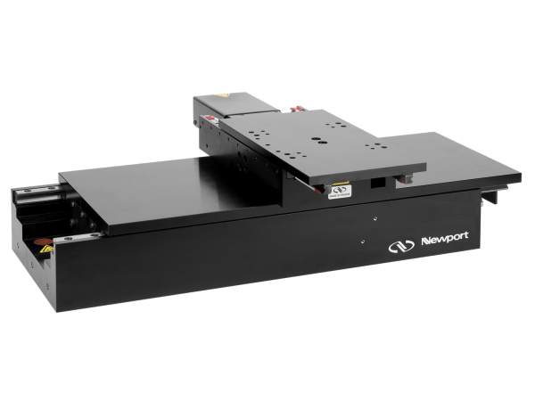
Positioners - Wafers & Reticles
MKS has the knowledge and expertise needed to address the most complex and demanding motion control applications. From traditional motorized linear stages to evolutionary air bearing systems, we have a solution to meet your needs.
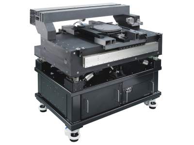
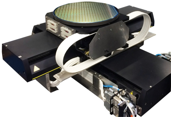
MKS DynamYX® Series Air Bearing Positioners are designed specifically for the semiconductor manufacturing industry. The positioners provide highest level of commercially available positioning performance and deliver high accuracy and high throughput. We have field-proven success with more than 1,000 DynamYX systems installed worldwide over the last 20 years.
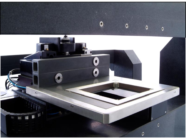
The DynamYX system is composed of 3 monolithic elements: a base, a guide and a carriage. The base serves as a reference surface for the moving elements. It’s made of precision-lapped granite, which offers the best flatness. Next is an L-shaped guide. This L-shape moves left and right along the rear of the reference surface base, for X-axis motion. The carriage then moves along with but perpendicularly to the L-shape for Y-axis motion – this is how XY movement is achieved. The L-shaped guide and carriage are made from silicon carbide ceramic. Advantages of this material include geometric stability, stiffness, and lower mass.
DynamYX employs air bearings for the smoothest, fastest, and most precise movements. The air bearings are created by the integration of pressure and vacuum into the L-shaped guide. The pressure areas and the vacuum areas are directly machined into the ceramic guide. Another benefit of this design is a very low profile. Ironless linear motors are used to generate the motion. Linear motors also provide the fastest, smoothest, and most precise motion, and they are also highly efficient in terms of heat dissipation and cooling. For X-axis movement, 1 or 2 motors are placed along the edge of the reference surface base. For Y-axis movement, the linear motor is built into the guide for the carriage to move along.
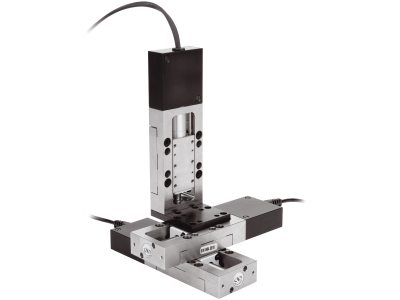
Similar to the DynamYX Series, MKS HybrYX® Series also has a granite base as the reference surface. But instead of the L-shaped guide and carriage of the DynamYX, the HybrYX utilizes a rigid, lightweight ceramic beam for X-axis motion and a ceramic carriage that slides along this beam for Y-axis motion. The beam is supported and guided at each end of the base by recirculating ball bearings for X-axis motion, while the carriage is pressure-vacuum preloaded to and guided along the beam for Y-axis motion. This blends the cost-effectiveness of mechanical bearings with the precision of a single plane air bearing carriage, which is an excellent combination of throughput, precision and value. The carriage is propelled by an ironless linear motor in the Y-axis, which is also similar to the DynamYX. The X-axis motor is also a linear motor, but iron core for the HybrYX.
- DynamYX® Datum® Air Bearing Positioning System: highest performance to provide the yield and throughput needed for the most demanding applications.
- DynamYX® GT Air Bearing Positioning System: outstanding performance for high-throughput applications with aggressive duty cycles.
- DynamYX® 300 Air Bearing Positioning System: cost-effective solution for high accuracy and dynamic performance.
- DynamYX® RS Air Bearing Reticle Positioning System: excellent performance for reticle inspection and repair applications.
- HybrYX® Hybrid Air & Mechanical Bearings Positioning System: combines the precision of air bearings with the cost-effectiveness of mechanical bearings for excellent value.
 DynamYX Datum |
 DynamYX GT |
 DynamYX 300 |
 DynamYX RS |
 HybrYX Hybrid |
|
|---|---|---|---|---|---|
| Travel Range | Up to 520 x 350 mm | Up to 520 x 350 mm | Up to 520 x 340 mm | Up to 290 x 155 mm | Up to 650 x 350 mm |
| Speed | 1 m/s | X: 800 mm/s, Y: 500 mm/s | 400 mm/s | 250 mm/s | X: 300 mm/s, Y: 600 mm/s |
| Peak Acceleration | X: 2 G, Y: 3 G | X: 1.2 G, Y: 2 G | X: 0.75 G, Y: 1.5 G | 0.25 G | X: 0.3 G, Y: 0.6 G |
| Accuracy (linear encoders) |
0.2 µm | 0.3 µm | 0.4 µm | 0.5 µm | 1.0 µm |
| Repeatability (long term) |
±25 nm | ±50 nm | ±50 nm | ±25 nm | |
| Straightness & Flatness (300-mm circle) |
0.3 µm | 0.4 µm | 0.6 µm | 0.6 µm | |
| Speed Stability | 0.05% | 0.1% | 0.1% | 0.1% | |
| Max Load Capacity | 30 kg | 30 kg | 15 kg | 20 kg | |
| Other Features | O-shaped ceramic guide Interferometer feedback option Z-Tip-Tilt-θ option for wafer chuck |
Z-Tip-Tilt-θ option for wafer chuck | Z-Tip-Tilt-θ option for wafer chuck | Extremely rigid ceramic reticle holder Cantilevered substrate located away from all moving elements |
Z-Tip-Tilt-θ option for wafer chuck |
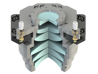
- ZT3 Z-Tip-Tilt-Theta Multi-Axis Positioner: active vertical, pitch, roll and yaw alignment of a wafer/chuck for challenging lithography and inspection applications.
| ZT3 | Z-Axis | Tip-Tilt | Θ-Axis | |
|---|---|---|---|---|
| Travel Range | 5 mm | ±2 mrad | ±3° | 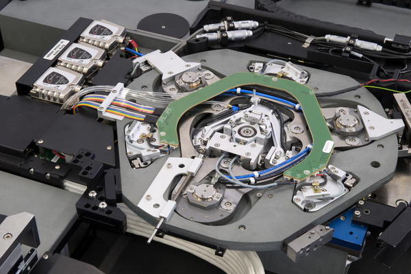 |
| Sensitivity | ±25 nm | 0.1 to 3 µrad | ||
| Step & Settle | 5 µm displacement in 40 ms settled to ±20 nm | |||
| Other Features | Optional piezo-driven Θ for 0.1 µrad sensitivity Lift-pin mechanism for easy wafer loading & unloading Air bearing Θ off-set stage, clamped after motion for ultimate stability |
|||
- IDL-LM Series Linear Motor Positioners: highest load capacity and speed of all linear motor stages for demanding production environments.
- XM-S Series Linear Motor Positioners: high sensitivity and outstanding trajectory accuracy in a compact, robust and cost-effective package.
 IDL-LM |
 XM-S |
|
|---|---|---|
| Travel Range | 100 to 1,200 mm | 50 to 350 mm |
| Speed | 2 m/s | 300 mm/s |
| Accuracy | ±2 to ±5 µm | ±0.2 to ±0.5 µm |
| Repeatability | ±0.25 to ±0.5 µm | ±0.03 to ±0.035 µm |
| Pitch | ±15 to ±65 µrad | ±25 to ±50 µrad |
| Yaw | ±15 to ±40 µrad | ±25 to ±40 µrad |
| Straightness & Flatness | ±0.75 to ±1.50 µm | |
| Max Load Capacity | 450 to 2,000 N | 100 to 300 N |
| Other Features | Ironless Linear Motor Recirculating ball bearings Industrial grade hard covers |
1-nm minimum incremental motion Ironless Linear Motor Crossed-roller bearings |
Wafer and Reticle Positioners Selection Guide
We summarize the recommended platforms for various applications below. Please use this as a reference guide and always contact us to discuss your application and requirement in detail so we can provide the best solution for you.
| DynamYX Datum | DynamYX GT | DynamYX 300 | DynamYX RS | HybrYX | IDL-LM | XM-S | |
|---|---|---|---|---|---|---|---|
| Wafer Inspection | ★★★ | ★★★ | ★★ | ★ | ★ | ★★ | |
| Optical Lithography | ★★★ | ★★★ | ★ | ||||
| Nano Imprint Lithography | ★★★ | ★ | ★ | ||||
| Memory Repair | ★★★ | ★★ | ★ | ||||
| Wafer Dicing | ★★ | ★★★ | ★★ | ||||
| Reticle Inspection & Repair | ★★★ | ||||||
| Mask Writing | ★ | ★★★ | ★ | ★★ | |||
| Wafer Bump Inspection | ★ | ★★ | ★★★ | ★★ |
Positioners - Optical Path
For applications such as Inspection and Lithography where the substrate is being moved, an optical path needs to be constructed to deliver the laser beam to targeted spots. MKS provides a variety of positioners that are ideal for building such an optical path, many of which are standard catalog products.
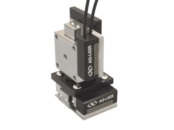
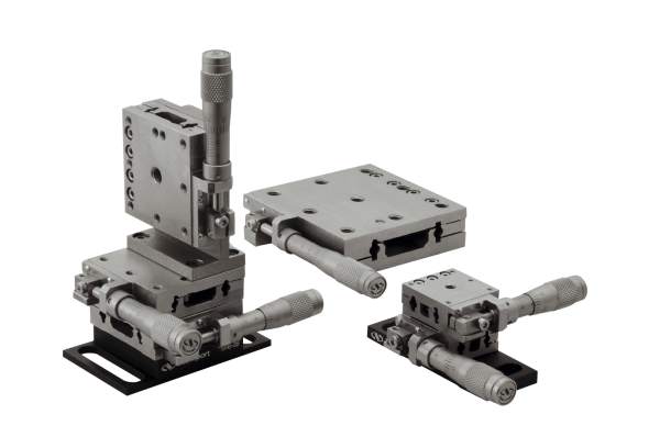
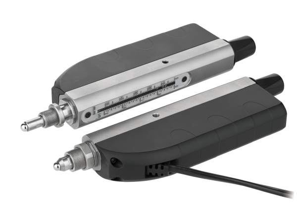
- Agilis™ Piezo Motor Linear Positioners: automated, fast nanometer-scale movement in a compact package.
- MFA Series Miniature Motorized Linear Positioners: high stability and stiffness in a compact package.
- SDS Series Low-Profile Steel Linear Positioners: lowest profile, sturdy motion and long-term stability designed for OEM applications.
 Agilis |
 MFA |
 SDS |
|
|---|---|---|---|
| Travel Range | 12 and 27 mm | 25 mm | 10 and 25 mm |
| Minimum Incremental Motion | 50 or 100 nm | 100 nm | |
| Angular Deviation | <200 µrad | Pitch: ±25 µrad, Yaw: ±30 µrad | Pitch: <200 µrad, Yaw: <150 µrad |
| Speed | 0.5 mm/s | DC: 2.5 mm/s, Stepper: 1 mm/s | |
| Accuracy | DC: ±0.7 µm, Stepper: ±0.9 µm | ||
| Repeatability | ±0.15 µm (w/ |
DC: ±0.15 µm, Stepper: ±0.2 µm | |
| Bearings | Ball | Ball | Ball |
| Material | Stainless Steel | Stainless Steel | Stainless Steel |
| Drive Type | Piezo Motor | DC Motor, Stepper Motor | Manual Micrometer |
| Other Features | Holding force locks position when idle Closed-loop version |
Side-mounted actuators Low profile, minimum footprint Non-influencing locking mechanism |
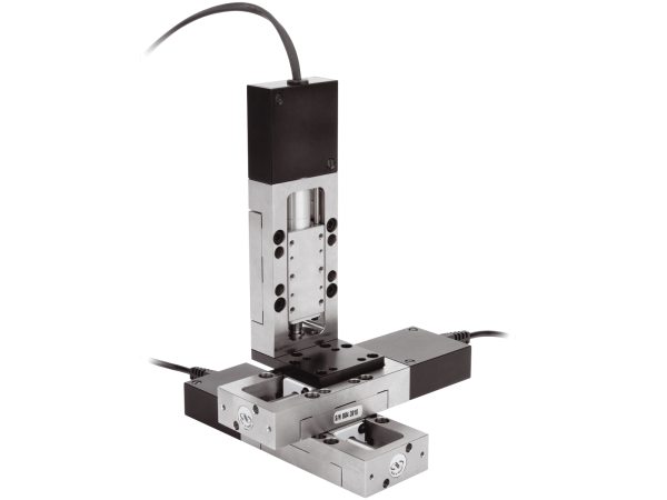
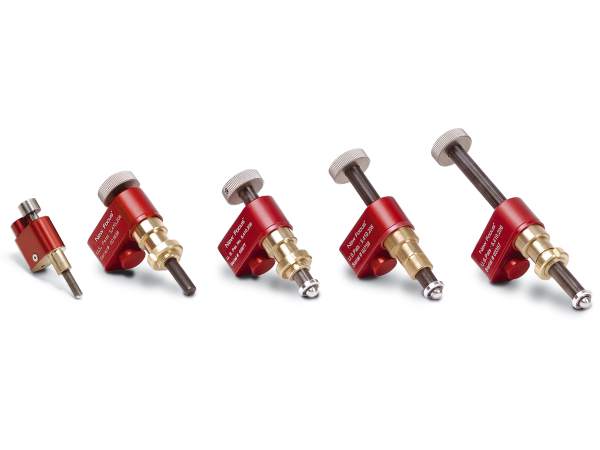
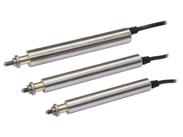
- Picomotor™ Series Piezo Actuators: nanometer-scale, automated motion in a compact package.
- TRA Series Actuators: the slim, lightweight, economic motorized upgrade for manual stages.
- LTA Series Precision Actuators: combines high accuracy, high speed and small minimum incremental motion.
 Picomotor |
 TRA |
 LTA |
|
|---|---|---|---|
| Travel Range | 12.7, 25.4 or 50.8 mm | 6, 12 or 25 mm | 25 or 50 mm |
| Minimum Incremental Motion | <30 nm | 100 or 200 nm | 50 or 100 nm |
| Axial Load Capacity | 22 or 13 N | 60 N | 120 or 50 N |
| Speed | 1.2 or 1 mm/m | 0.4 mm/s | 1 or 5 mm/s |
| Accuracy | ±1.5 to ±2.5 µm | ±1.2 or ±2.2 µm | |
| Repeatability | ±1.25 µm | ±0.3 µm | |
| Other Features | No movement when power is off Manual adjustment knob |
- Agilis™ Piezo Optical Mounts: automated, high sensitivity optical adjustments.
| Agilis | ||
|---|---|---|
| Optic Diameters | 0.5 and 1 in. | 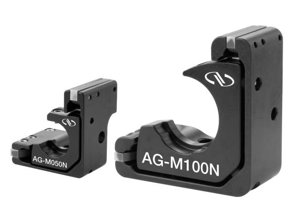 |
| Angular Range | ±2° in 2 axes | |
| Adjustment Sensitivity | 1 or 2 µrad | |
| Speed | 0.5 or 0.75 °/sec | |
| Other Features | Limit switch version for repeatability True set-and-forget stability |
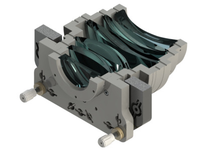
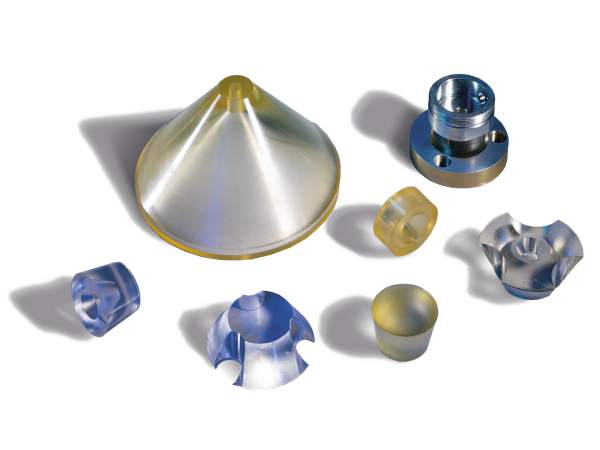
Complex Optics & Optical Assemblies
MKS has a very experienced team of lens designers, opto-mechanical engineers and physicists that specialize in optical design and development. We are more than just a supplier of optical components – MKS can be your partner to deliver optical solutions for your needs. We can provide high precision optical assemblies – for example, lens assemblies for lithography. We can also build complete integrated solutions of optics, opto-mechanics and electronics, such as an optical path system for an inspection scanning application.
We specialize in the design of thin film coatings for laser optics whether it be reflective, anti-reflective, partially reflective, high power and other types. The trend with semiconductor manufacturing is going towards DUV and EUV as electronic devices become smaller and smaller, and we have much experience with coatings down to 193 nanometers. If you think you might need to go lower than that, please talk to us to see how we might be able to help you. In addition to providing traditional optical shapes and coatings, MKS can also produce complex optical shapes, such as freeform optics, highly convex or concave optics, truncated optics and lightweight optics. We also have the capability of placing multiple coating types on a single optical component.
MKS will design a custom solution to meet your application's requirements, and we can handle build-to-print or build-to-specs. With our world class manufacturing capabilities, we are able to scale quantities as needed and also provide cost-effective high volume production.
State-of-the-Art Optics Manufacturing Technologies
| Materials | Fabrication | Coatings |
|---|---|---|
|
|
|
Advanced Metrology and Testing
| Coated Optics Testing | Alignment Turning | HALT/HASS |
|---|---|---|
|
|
|
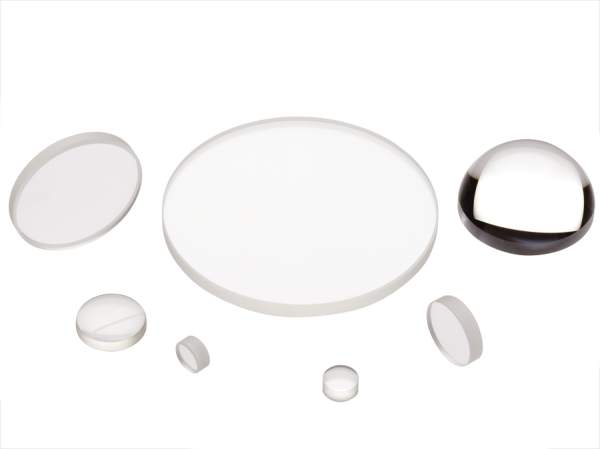
Catalog Optics
- Precision Polished Aspheric Lenses: combine the performance of multiple spherical lenses to reduce the optical path length and number of components.
- Singlet Spherical Lenses: good performance and value over broad spectral ranges.
- Cylindrical Lenses: good performance and value over broad spectral ranges.
 Aspheric |
 Spherical |
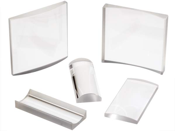 Cylindrical |
|
|---|---|---|---|
| AR Coating Wavelengths | 430-700 nm 650-1000 nm |
245-440 nm 430-700 650-1000 1000-1550 |
245-440 nm 430-700 650-1000 1000-1550 |
| Avg. Reflectivity per Coated Surface | <0.5% | <0.5% | <0.5% |
| Diameters | 15 to 50 mm | 0.25 to 3 in. | ¼ x 1 in. to 2 x 2 in. rectangular 12.5 to 25 mm round |
| Effective Focal Lengths | 11.3 to 50 mm | 0.4 mm/s | 1 or 5 mm/s |
| Shapes | Plano-Convex Bi-Convex |
Plano-Convex Bi-Convex Plano-Concave Bi-Concave |
Plano-Convex Plano-Concave |
| Substrate Materials | L-BAL35 Glass | N-BK7, UV Fused Silica | N-BK7, UV Fused Silica |
| Other Features | Reduced Spherical Aberration Computer-optimized for diffraction limited performance |
- Broadband Metallic Mirrors: good performance and value over very broad spectral ranges.
| Wavelengths | 250-600 nm* | 450-700 nm | 480-20000 nm | 650-20000 nm | |
|---|---|---|---|---|---|
| Coatings | UV Aluminum | Aluminum | Silver | Gold | 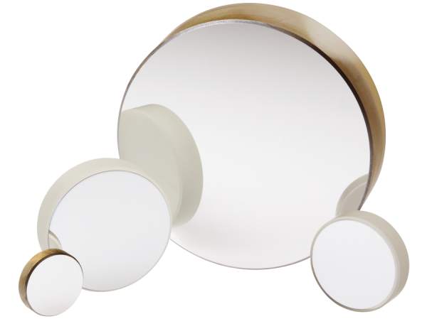 |
| CW Damage Threshold | 100 W/cm2 | 100 W/cm2 | 1000 W/cm2 | 200 W/cm2 | |
| Reflectivity | >90%* | >93% | >96% | >96% | |
| Diameters | 0.5 to 8 in. | ||||
| Other Shapes | Square, Elliptical, D-shaped, Concave | ||||
| Substrate Materials | Borofloat 33, Zerodur | ||||
| Other Features | Insensitive to polarization and AOI | ||||
| * Can perform at 193 nm with lower reflectivity | |||||
Diffraction Gratings
- Diffraction Gratings: separates polychromatic light into various wavelengths at slightly different angles.
| Diffraction Gratings | ||
|---|---|---|
| Master Types | Ruled, Holographic, Echelle | 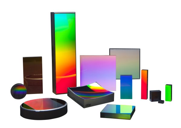 |
| Grating Types | Reflection, Transmission, Grism (grating prisms) | |
| Shapes | Plano, Concave | |
| Grooves per millimeter | 30 to 5,880 | |
| Spectral Regions | Various, including 193 and 248 nm and other multiple high-orders within UV | |
| Sizes | 2 x 2 mm to 320 x 420 mm | |
| Other Features | High efficiency Very low Rowland ghost High resolving power |
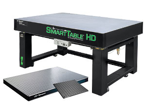
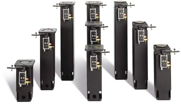
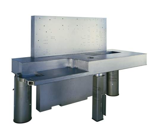
Isolation - Vibration Control
MKS sets the industry standard for vibration control with the very first steel-clad, honeycomb core table that was designed a few decades ago to isolate laser experiments from vibration. Over the years we’ve built a comprehensive offering of optical tables, workstations, isolators, breadboards, and everything vibration control. MKS also has extensive capabilities to design and build custom solutions, such as non-standard geometries, less magnetic or non-magnetic table tops and cleanroom- or vacuum-compatible structures. We can also provide some services like testing and analysis.
- NewDamp™ Elastomeric Vibration Isolators: supports and dampens high acceleration amplitudes produced by high through wafer positioners.
| NewDamp | ||
|---|---|---|
| Minimum Load per Isolator | 6 to 45 kg | 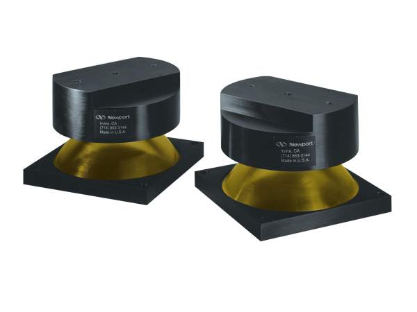 |
| Load Capacity per Isolator | 8 to 200 kg | |
| Loss Factor | 0.5 to 0.8 in 10-100 Hz range | |
| Height | 1.32 to 3.28 in. | |
| Base Size | 2.4 x 2.4 to 4.5 x 4.5 in. | |
| Constant natural frequency design | Fast settling times Cleanroom compatible Breadboard, Microlock and X95 compatible |
Custom Isolation Solutions
- Elastomer dampers
- Tuned solution specific to machinery characteristics such as load, shock response and resonance modes
- Similar technology as NewDamp™
- Can be built into equipment isolation supports and custom machinery feet
- Pneumatic isolators
- Custom-designed isolation platform, available individually or in sets
- Cleanroom version available
- Scalable quantities
Custom Honeycomb Structure Solutions
- Design assistance on construction or use of special tables, systems or structures
- Custom lengths, widths and hole patterns
- Laminar airflow and vacuum pull designs
- Cleanroom or vacuum compatible
- Special materials available, including nonmagnetic
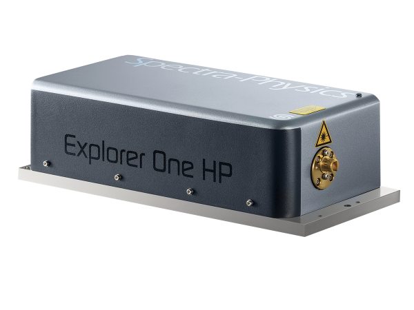
Lasers
As electronic devices become smaller and smaller and transistor density increases, lasers will play an increasingly important role in semiconductor manufacturing. MKS offers a variety of lasers to meet your application requirements.
Nanosecond Lasers
- Explorer® One™ Compact Nanosecond Lasers: the most compact UV and green nanosecond lasers in its class with high peak power and short pulse widths.
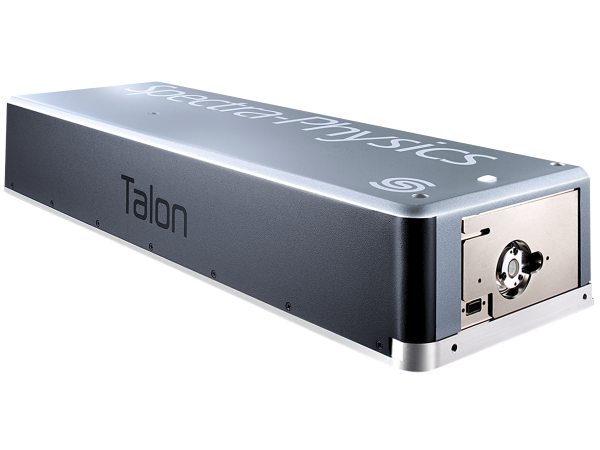
- Talon® Nanosecond Lasers: superior combination of performance, reliability and cost.
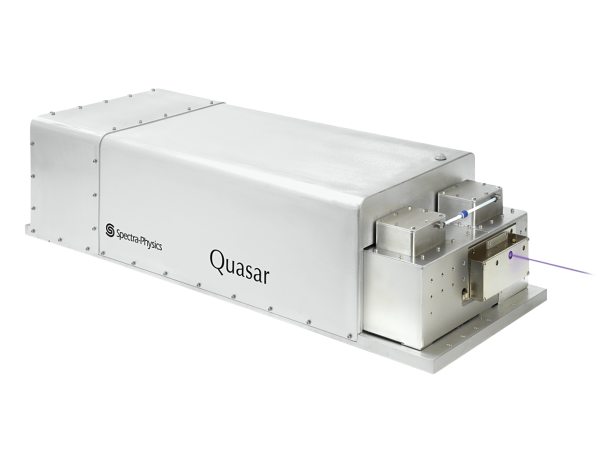
- Quasar® High-Power Nanosecond Lasers: highest power UV and green hybrid fiber lasers, with programmable pulses, for highest throughput and quality in the industry.
- SPFL-532 Short-Pulsed Green Fiber Lasers: high repetition rates with adjustable short pulse widths for fine materials processing.
 Explorer One |
 Talon |
 Quasar |
 SPFL-532 |
|
|---|---|---|---|---|
| Wavelengths | UV or Green | UV or Green | UV or Green | Green |
| Power | UV: Up to 120 mW or >6 W Green: Up to 5 W |
UV: Up to >45 W Green: Up to >40 W |
UV: Up to >80 W Green: Up to >95 W |
Up to >40 W |
| Pulse Width | UV: <5 ns or <10 to <15 ns Green: <10 to <15 ns |
UV: <25 or 40 ns Green: <25 ns |
<2 to >100 ns | 3-6 or 9-50 ns |
| Repetition Rates | UV: Single shot to 5 kHz or 500 kHz Green: Single shot to 500 kHz |
0 to 500 kHz | 0 to 3.5 MHz | Single Shot to 2 MHz |
| Max Pulse Energy | UV: Up to 120 µJ or >200 µJ Green: Up to 200 µJ |
UV: Up to >500 µJ Green: Up to 1000 µJ |
UV: Up to >400 µJ Green: Up to >475 µJ |
Up to 100 or 180 µJ |
| Other Features | Very compact, lightweight air-cooled designs | Laser/controller in single, compact package 24/7 industrial reliability E-Pulse™ technology for superb stability |
24/7 industrial reliability TimeShift™ technology for pulse control |
24/7 industrial reliability TimeShift™ technology for pulse control |
| Use | ✓ Inspection and Metrology ✓ Marking |
✓ Low-K Grooving ✓ Dicing ✓ Marking ✓ Package Cutting and Drilling |
✓ Low-K Grooving ✓ Dicing ✓ Package Cutting and Drilling |
✓ Marking |
Picosecond Lasers
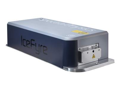
- IceFyre® Picosecond and Femtosecond Lasers: exceptional performance and unprecedented versatility at industry-leading cost-performance.
| Picosecond | Femtosecond | ||||
|---|---|---|---|---|---|
| Wavelengths | UV | Green | IR | UV | 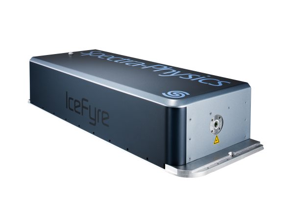 |
| Power | Up to >50 W | ||||
| Pulse Width | <12 ps | <15 ps | <500 fs | ||
| Repetition Rates | Single Shot to 10 MHz | Single Shot to 3 MHz | |||
| Max Pulse Energy | Up to >40 µJ | Up to >60 µJ | Up to >200 µJ | Up to >50 µJ | |
| Other Shapes | 24/7 industrial reliability TimeShift™ technology for pulse control Laser/controller in single, compact package |
||||
| Use | ✓ Low-K Grooving ✓ Dicing ✓ Package Cutting and Drilling |
||||
Femtosecond Lasers
- Spirit® High Power Femtosecond Lasers: high average power, high pulse energy and high repetition rates for increased throughput.
| Wavelengths | Green | IR | |
|---|---|---|---|
| Power | >50 W | Up to >30 W or >140 W | 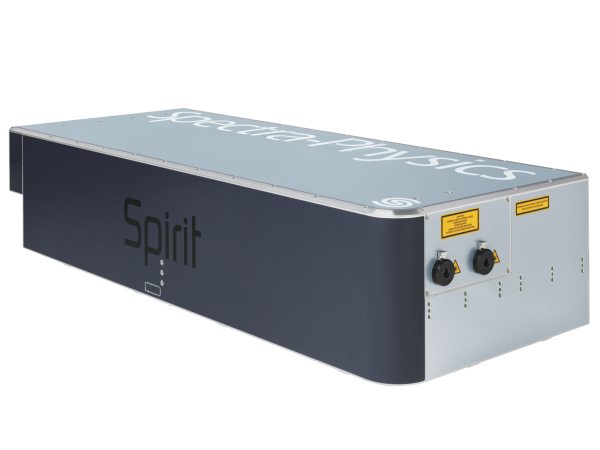 |
| Pulse Width | <400 fs | <400 fs or <500 fs | |
| Repetition Rates | Single shot to 30 MHz | Single shot to 1 MHz or 30 MHz | |
| Max Pulse Energy | >50 µJ | Up to >600 µJ or >120 µJ | |
| Stability | <2% | ||
| Other Shapes | User-configurable burst mode | ||
| Use | ✓ Dicing | ||
Laser Power Sensors
MKS offers a comprehensive portfolio of power sensors, and the ones shown here are examples of sensors designed to measure optical output power of short pulsed lasers such as Talon and IceFyre that operate in nano-second and pico-second pulse widths. These sensors have a very high damage threshold to withstand the high optical peak power delivered by each pulse in the UV and IR wavelength range.
- Laser Thermal Power Thermal Sensors: very high damage thresholds for hundreds of watts power measurement.
| F150(200)A-CM-16 | 30(150)A-SV-17 | F80(120)A-CM-17 | ||
|---|---|---|---|---|
| Spectral Range | 0.248-9.4 µm | 0.19-11 µm | 0.248-9.4 µm | 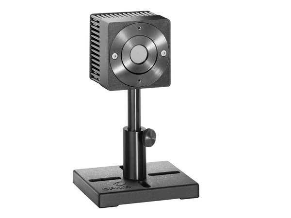 |
| Power Range | 300 mW - 200 W | 100 mW - 150 W | 100 mW - 120 W | |
| Energy Range | 50 mJ – 200 J | 50 mJ – 300 J | 50 mJ – 200 J | |
| Max Avg Power Density | 35 kW/cm2 | 60 kW/cm2 | 35 kW/cm2 | |
| Max Energy Density (2 msec) | 45 J/cm2 | 50 J/cm2 | 45 J/cm2 | |
| Aperture | Ø16 mm | Ø17 mm | Ø17.5 mm | |
| Response Time | 3 sec | 1.7 sec | 2 sec | |
| Use | Not water-cooled | |||
The recommended products above are the most popular models for semiconductor manufacturing. We have a lot more than these and you can use our online tools to find the ones that best fit your requirements.

For additional insights into photonics topics like this, download our free MKS Instruments Handbook: Principles & Applications in Photonics Technologies
Request a Handbook