Power Electronics
Power electronics is a category of products playing a central role in the ongoing technological transformation of modern society. These are devices which convert, control and condition electrical power. Some examples of power electronics devices are diodes, rectifiers, inverters, converters, choppers and transistors. Since the dawn of electronic devices, silicon has been the predominant semiconductor material, and it continues to dominate power electronics devices. However, silicon-based power electronics have inherent limitations that restrict their performance in more demanding applications.

Updated: 6/16/2006
Expanding Power Electronics Beyond Silicon
One development requiring higher performing power electronics is the growing adoption of electric vehicles (EVs) and expectations of longer driving ranges and faster charging times. Another trend calling for more advanced power electronics is the shift towards renewable energy sources which rely on efficient power conversion and reduced power losses. Consumer electronics and telecom also demand power electronics that can manage higher power densities and faster switching speeds while providing better thermal management.
Silicon-based power electronics are able to serve a portion of the applications described above, but they are mostly suitable for applications such as home appliances, power tools, and less demanding data center functions—for these types of applications, lower to mid-range switching frequencies are suitable, and cost often takes precedence over performance or form factor. But beyond mid-range switching frequencies, silicon-based power electronics fall short due to the inherent bandgap of silicon. Semiconductors with wider bandgaps than silicon are therefore needed because they deliver higher power, switching frequency, operating temperature, and switching voltages, along with better efficiency. Two materials in particular with wide bandgaps have already proven their worth for power electronics: silicon carbide (SiC) and gallium nitride (GaN). The bandgaps of SiC and GaN are over two and three times greater in electron volts (eV) than silicon's.
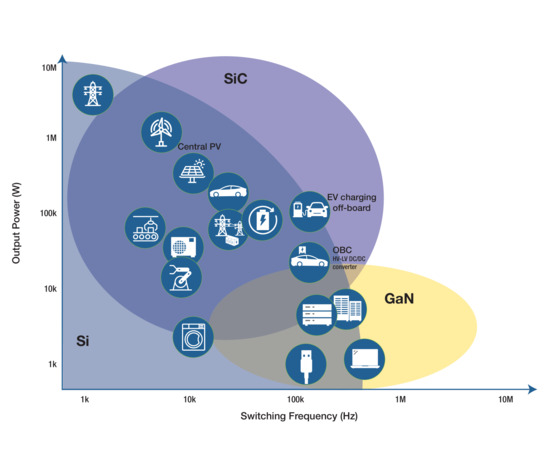
SiC-based power electronics are ideal for high-power/high-switching frequency applications. For instance, the potential for EVs with SiC-based power electronics includes longer driving ranges, faster charging times, and lighter vehicle weight. Also, more compact and more efficient energy storage systems may be possible with SiC. While GaN is limited to medium-power applications, it offers the highest operating frequency among these technologies. As a result, GaN-based power electronics enable new possibilities in consumer electronics and telecom, including widespread wireless charging and faster communication speeds.
All of these technologies overlap in roughly the mid-power/mid-frequency space, creating a "competing zone" among them. In this arena, silicon may be preferred when cost is the primary concern. But when higher performance, better efficiency, or smaller-sized products are desired, SiC or GaN should be considered.
SiC and GaN Manufacturing Challenges
Manufacturing of traditional silicon-based power electronics is well known and established, but SiC- and GaN-based power electronics presents new and more difficult challenges.
SiC as a raw material is much more costly than silicon is, and finished devices are about three times more expensive. SiC wafers are more brittle, thinner and smaller than silicon wafers are, so handling SiC wafers during the manufacturing process is more delicate, complex, and expensive.
GaN wafers are even more brittle, thinner and smaller than SiC wafers, so handling GaN wafers is even more complicated and costly than handling SiC wafers. Interestingly, however, GaN-based products can be cheaper than those made of silicon for equivalent power conversion specifications—this is due to GaN's higher efficiency, lower operating costs and smaller footprint.
While SiC and GaN wafer fabs share many steps used in silicon wafer manufacturing, there are some notable differences. For example, SiC and GaN wafer ingot slicing is typically performed by lasers instead of mechanical diamond saws to improve wafer yields and lower costs by reducing material waste and scrap. Also, an existing silicon wafer processing line cannot be used as-is on SiC or GaN wafers, partly because wafer handling equipment developed for silicon may not be appropriate for SiC or GaN wafers.
Newport has decades of experience with silicon wafer processing from front-end to back-end and can work with you to develop and build the right solution for your SiC or GaN needs.
| Si (base case) | SiC | GaN | |
|---|---|---|---|
| Device Cost | $ | $$$ | $ |
| Typical Maximum Wafer Diameter | 300 mm | 200 mm | 150 mm |
| Typical Wafer Thickness | 0.4-0.5 mm | 0.35-0.5 mm | 0.25-0.3 mm |
| Manufacturing Complexity | ⚙ | ⚙⚙ | ⚙⚙⚙ |
The MKS Advantage for SiC and GaN Manufacturing
With decades of experience in silicon wafer processing from front-end to back-end, MKS has a deep understanding of the challenges involved in designing and manufacturing power electronics. That experience is built into specific product features designed to address the demands of SiC- and GaN-based power electronics manufacturing. Some of these features are described here.
Lasers
Lasers Provide Advantages Over Traditional Processes
Lasers are superior to traditional mechanical methods such as blades and drills in applications including ingot slicing, scribing, grooving, dicing and marking. For example, the time-consuming process of slicing a SiC ingot with a mechanical diamond saw can waste up to 75% of the material. Because SiC is significantly harder than silicon, a blade wears faster, leading to increased replacement costs and more frequent downtime. By comparison, laser ingot slicing for SiC and GaN results in minimal material loss, and there is no tool wear. And by employing the appropriate laser and slicing methodology, laser ingot slicing can be considerably faster than mechanical slicing.
Spectra-Physics lasers are high-precision instruments that cut and drill accurately and repeatably on the order of microns — a level of consistency that mechanical tools cannot reliably match. SiC and GaN wafers are already more brittle than silicon and must be handled more delicately, and as SiC and GaN devices become more complex, they might be even more difficult to produce solely through mechanical means. In addition to the high precision, lasers also offer more flexible patterns for cutting and drilling, which further enables more complex designs and higher performing devices to be made.
Another important advantage that lasers present over traditional processes is the quality of their results. With slicing, scribing, grooving and dicing, lasers produce fewer burrs and less damage to the surrounding areas than mechanical cuts do. This results in higher manufacturing yields, as less of the material is wasted. Laser operations also produce fewer latent defects and cracks compared to mechanical operations, improving product quality and field reliability — not all such defects are caught before products leave the factory. And like laser ingot slicing, laser scribing, grooving, dicing and marking are contact-free operations, so there is no tool wear, and the replacement downtime is exceedingly infrequent compared to mechanical methods.
Taken all together, SiC and GaN processing with lasers will enable the production of devices that are mainstream enough to complement and compete with silicon-based electronics.
High-Power Nanosecond UV Lasers
The Spectra-Physics Talon® Ace UV100 is the highest-powered single-mode UV laser in the industry, with the lowest cost-per-watt and cost of ownership for high-power nanosecond UV lasers. With high throughput and precision output quality, this laser is ideal for scribing, grooving, and dicing SiC and GaN wafers. Designed to provide 24/7 industrial reliability, the laser and controller are integrated into a single, compact package.
Nanosecond UV and Green Lasers
For demanding SiC and GaN manufacturing applications, Spectra-Physics Talon® lasers deliver high performance at a competitive cost. The UV version is well-suited for marking, scribing, grooving, and dicing, while the green wavelength supports wafer dicing and ingot slicing. Based on Spectra-Physics’ It’s in the Box™ design, the laser and controller are integrated into a single, compact package, and Talon is manufactured to provide 24/7 industrial reliability.
Ultrashort Pulsed Lasers
For SiC and GaN manufacturing where cut quality is critical, ultrashort pulse lasers deliver the cleanest cuts and smallest heat affected zones (HAZ). Spectra-Physics IceFyre® lasers set a new standard for picosecond micromachining. For scribing, grooving, and dicing, the UV version is ideal, while the green version can also be used for grooving and dicing. The IR version of IceFyre works best for ingot slicing. IceFyre® FS femtosecond lasers deliver higher quality results than the IceFyre picosecond laser, making them the choice for the most demanding ultrashort pulse applications. The UV and IR versions of IceFyre FS work extremely well for scribing, grooving, and dicing, and the IR version can also perform ingot slicing. Based on Spectra-Physics’ It’s in the Box™ design, these lasers integrate the laser and controller into a single, compact package and provide 24/7 industrial reliability.
Selecting a Laser for Power Electronics Processing
For marking, the Talon UV nanosecond laser works well, as does the Explorer® One UV and green nanosecond lasers. And even though there’s no check-mark in the table for it, Talon Ace can also perform marking, although that probably wouldn’t be its primary application. Ingot slicing can be performed with the IR version of our IceFyre picosecond and IceFyre FS femtosecond IR lasers, or with the green version of the Talon nanosecond laser. Scribing is a process to create deep cuts in the substrate material – like an SiC or GaN wafer – in preparation for dicing. A UV wavelength is the recommended choice for scribing, making Talon Ace, Talon, IceFyre, and IceFyre FS the strongest options. The Spirit green femtosecond laser and the IR version of the IceFyre FS are also well suited for scribing. Grooving is done to make shallow cuts to precise target depth and desired features. Examples include v-grooves and also possibly removal of thin film. A UV wavelength is again the recommended choice for grooving. Other lasers that can perform grooving well are the green versions of the IceFyre and Spirit, and also the IR version of the IceFyre FS.
| Talon® Ace™ (ns) | Talon (ns) | IceFyre® (ps) | IceFyre FS (fs) | Spirit® (fs) | Explorer® One™ (ns) | ||||||
|---|---|---|---|---|---|---|---|---|---|---|---|
| UV | UV | Green | UV | Green | IR | UV | IR | Green | UV | Green | |
| Marking | ✓ | ✓ | ✓ | ||||||||
| Ingot Slicing | ✓ | ✓ | ✓ | ||||||||
| Scribing | ✓ | ✓ | ✓ | ✓ | ✓ | ✓ | |||||
| Grooving | ✓ | ✓ | ✓ | ✓ | ✓ | ✓ | ✓ | ||||
| Dicing | ✓ | ✓ | ✓ | ✓ | ✓ | ✓ | ✓ | ✓ | |||
| Via Hole Drilling | ✓ | ✓ | ✓ | ✓ | |||||||
Motion Control
Nanometer Scale Wafer Positioners
Wafer positioning performance for processes including lithography, inspection and dicing can be particularly challenging, often with sub-micron and even nanometer scale accuracy and repeatability required. This precise level of operation must also be delivered quickly, with speeds up to 1 m/s, to maximize throughput.
To address the wafer positioning demands of the semiconductor manufacturing industry, MKS developed the Newport DynamYX® series positioner, a high-throughput, high-accuracy solution based on air bearing and linear motor technology. With over 20 years of field-proven success in more than 1,000 systems installed worldwide, DynamYX provides the highest level of commercially available positioning performance. MKS also offers the Newport HybrYX® series positioner, a hybrid air and mechanical bearings system with linear motors that delivers high throughput and accuracy.
All DynamYX and HybrYX systems are custom-designed, meaning techniques and solutions developed for silicon processing can be adapted for SiC and GaN processing.
Air Bearing Positioning Systems
Newport DynamYX is a high-throughput, high-accuracy positioning solution that delivers the highest level of commercially available positioning performance. Featuring air bearing and linear motor technology, DynamYX provides sub-micron accuracy and nanometer scale repeatability at speeds of up to 1 m/s for applications including wafer and reticle inspection, lithography, mask writing, and wafer dicing. Over 1,000 DynamYX systems have been installed worldwide.
Another type of Newport air bearing platform is the HybrYX-HD with Soft Isolation, which uses an air bearing for one axis of motion, mechanical ball bearings for the other axis, and linear motors for both axes. HybrYX-HD can deliver speeds of up to 1.5 and 2 m/s, sub-micron accuracy, and nanometer-scale repeatability. More economical than DynamYX, HybrYX-HD with Soft Isolation is ideal for wafer dicing and may also be used for wafer inspection.
Industrial Grade Linear Positioners
The Newport IDL-LM series are industrial-grade positioners with an ironless linear motor and recirculating ball bearings, delivering the highest speed and load capacity of any linear motor stage in the lineup. With an accuracy on the order of microns and sub-micron repeatability, these positioners are excellent for SiC and GaN manufacturing. Built for production environments, all IDL-LM positioners include a hard top cover, wear-resistant flexible side bands, air purge, and a directed debris path.
Wafer and Reticle Positioners Selection Guide
Below is a selection guide for the various applications and our recommended motion platforms. Please keep in mind that this is only a guide, and we’d love to discuss your application and requirements in detail with you so we can help provide the best solution for you. For wafer inspection, our DynamYX systems deliver best-in-class performance, and HybrYX offers strong price-to-performance value. The IDL and XM Series linear stages can also be used depending on your requirements. For lithography, reticle inspection and repair, and mask writing, DynamYX is the recommended platform. For wafer dicing, HybrYX is ideal because of its outstanding price-to-performance value, but you can also consider the DynamYX and the IDL stages.
| DynamYX® | HybrYX® | IDL | XM | |
| Wafer Inspection | ★★★ | ★ | ★ | ★★ |
| Lithography | ★★★ | |||
| Wafer Dicing | ★★ | ★★★ | ★★ | |
| Reticle Inspection & Repair | ★★★ | |||
| Mask Writing | ★★★ |
Beam Analysis
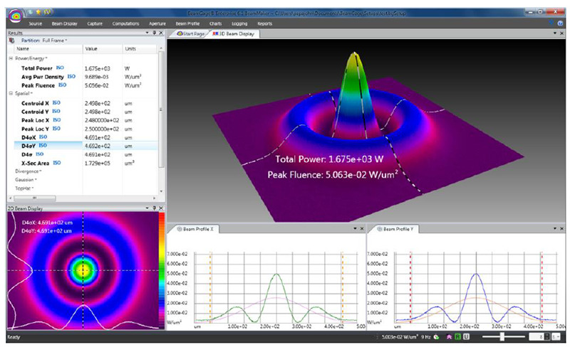
Even with the advantages that lasers have over traditional tools, laser systems can still degrade over time. Some causes of degradation include thermal effects on a laser system's internal components, vibrations or shock, and debris near the processing site. These issues could affect laser performance in a number of ways. First, output power may be reduced, causing the laser to be less efficient. Beam focus and profile can also shift, causing cuts or drills to miss their target, go too deep, produce poor quality results, or damage surrounding material.
To maintain the highest quality when manufacturing SiC and GaN wafers and to minimize production downtime, laser beams should be monitored regularly with appropriate instruments, such as Ophir® power sensors, power meters, and beam profilers, that can characterize the laser at its maximum output power level.
Laser Thermal Power Sensors
Newport offers Ophir® laser thermal power sensors, several of which can measure the optical output power of short- and ultrashort-pulsed lasers such as Talon Ace, Talon, and IceFyre. Each sensor is built with a high damage threshold to withstand the peak optical power delivered by each pulse. Also included with each sensor is a standard 1.5-meter cable to connect to a power meter or PC.
- Spectral ranges from UV to mid-IR
- Power ranges up to a few hundred Watts
- Apertures from 16 to 30 mm diameter
- Response times 1 second or less for most applications
Beam Profiling Cameras
Camera-based systems are a reliable way to analyze beam profiles with high precision. Ophir beam profiling cameras allow real-time viewing and measuring of a laser’s structure in high resolution. Camera-based systems can also measure cross-sectional intensity of the laser and provide a complete 2-dimensional view of the laser mode.
- Spectral ranges from UV to mid-IR
- High-resolution, real-time viewing
- Highest accuracy measurements
- User-friendly BeamGage software with extensive analytical features included
Optics
High-Energy Laser Optics
Dozens of Newport standard catalog optics are designed to operate with high-energy lasers such as those used in SiC and GaN manufacturing. Mirrors, lenses, beam splitter cubes, and waveplates are available in various sizes, with substrate materials and coatings optimized for 355, 532, and 1064 nm wavelengths. These optics withstand laser fluences of single to tens of Joules of pulsed energy per square centimeter, supporting a wide range of SiC and GaN manufacturing applications.
- Mirrors, lenses, beam splitter cubes, waveplates
- Optimized for 355, 532 and 1064 nm wavelengths
- Extensive ultrafast optics selection
- High LIDT (Laser Induced Damage Threshold)
Opto-Mechanics
Opto-Mechanical Components
When optics are part of a laser system, they must be precisely positioned and held securely over extended periods. Newport offers a complete line of optomechanical components for precision laser and optical system builds. Hundreds of optical mounts and positioners at various levels of performance and cost are readily available.
- Mirror mounts, lens positioners, and other optical mounts
- Linear and rotary positioners
- Post and pedestal assemblies
- Stainless steel and aluminum
Vibration Control
Vibration Isolation
MKS offers industry-leading Newport vibration isolation solutions that can be integrated into SiC and GaN wafer positioning systems. Our NewDamp™ series of elastomeric isolators, available as standard catalog products or custom designs, is ideal for supporting and damping the high acceleration amplitudes produced by very high-throughput wafer positioners such as the Newport DynamYX. Custom pneumatic isolator solutions are also available individually or in sets. For custom vibration isolation, MKS will work with you to understand your machinery characteristics such as load, shock response and resonance modes, and the isolators can be built into your equipment’s isolation supports.
- Elastomeric and pneumatic isolators
- Standard catalog products or custom solutions tuned specifically to your system
- Can be built into equipment isolation supports
- Scalable quantities
Resources
Powering SiC-GaN Semicon Mfg Brochure(11 MB, PDF)