Semiconductor Inspection
In this application note, we provide a brief description of the basics of wafer and reticle inspection techniques and discuss the characteristics of current inspection tools.
Scanning Defect Inspection
Prior to starting production, bare wafers are qualified at the wafer manufacturer and again upon receipt by the semiconductor fab. These qualifications locate, map, and differentiate pre-existing defects from those arising in the IC manufacturing process. Only the most defect-free wafers are used in production, and their pre-production defect maps allow manufacturers to track regions that are likely to result in poorly functioning chips. Bare or non-patterned wafers are also measured before and after being subjected to a passive or active process environment to determine a baseline for particle contributions from a given process tool.
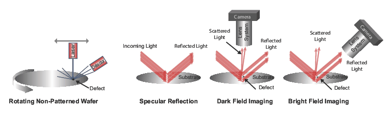
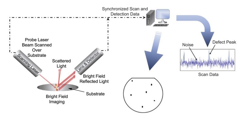
Device manufacturers use optical detection systems to inspect wafers and masks for particles and other types of defects and to determine the position of these defects in an X-Y grid on the wafer. The basic principle used for defect detection on non-patterned wafers is relatively simple. A laser beam is radially scanned over the surface of a rotating wafer to ensure that the beam is projected onto all parts of the wafer surface. The laser light is reflected from the surface as it would be from a mirror, as is shown in Figure 1. This type of reflection is referred to as specular reflection. When the laser beam encounters a particle or other defect on the surface of the wafer, the defect scatters a portion of the laser light. Depending on the illumination arrangement, the scattered light can be detected directly (dark-field illumination) or as a loss in intensity in the reflected light beam (bright-field illumination). The rotational position of the wafer and radial position of the beam define the position of the defect on the wafer surface. In wafer inspection tools, the light intensity is electronically recorded using a PMT or CCD and a map of the scattered or reflected intensity over the wafer surface is generated, as shown in Figure 2. This map provides information on defect size and location and on the condition of the wafer surface due to issues such as particle contamination. This method requires highly accurate and repeatable rotary and linear motion control of the wafer stage and optical components.
In general, dark-field inspection is preferred for non-patterned wafer inspection since high rastering speeds are possible and this enables high wafer throughput. Patterned wafer inspection is a much slower process. It may use bright-field and/or dark-field imaging, depending on the application. Note that the complexity of scattering from patterned surfaces reduces the overall photon flux to the detector, resulting in longer integration periods for wafer inspection.
Sub-100 nm inspection tools are currently used in manufacturing environments to provide quality assurance on incoming wafers and for process tool monitoring and qualification for high volume manufacturing. These tools employ the same basic operating principles as tools designed for larger scale defect detection but use DUV illumination-enhanced optical systems. Sophisticated image analysis algorithms are claimed by some manufacturers to achieve sub-20 nm sensitivity. As might be expected, a high degree of precision and accuracy is required in the motion control of the wafer stage and the optical components in systems used in these applications.
As inspection tools are required to sense and quantify ever smaller particles, the impact of factors such as surface microroughness (haze) begins to influence the detectability of small particles owing to reductions in the SNR of the scattered light signal. Sub-100 nm inspection for non-patterned wafers is complicated by issues of scale with SNR being a critical parameter in determining an inspection system's detection limits for particles and other defects on wafer surfaces. Surface chemical contamination from sources such as ambient humidity can also contribute to reductions in SNR. To help counter such effects, inspection tools for sub-100 nm defect detection employ highly sophisticated optical spatial filtering, analysis of polarization of the scattered signal, and specialized signal processing algorithms to detect defects in the presence of surface haze.
Topography Inspection
Bare wafer topography is measured for many reasons. For example, a wafer can bend or the chuck (either electrostatic or pneumatic) that supports a wafer can produce indentations in the wafer at points of contact. Such deformations can affect pattern imaging at nm scales. Extremely precise interferometric tools have been developed to measure such variations in wafer shape prior to processing.
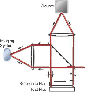
The basic design used to measure topography on bare wafers is similar to the Fizeau interferometer shown in Figure 3. This interferometric technique compares the wafer to a reference wedge (or reference flat) of very high quality and flatness. The wedge angle ensures that reflections from the first surface of the flat do not contribute to the interferometric signal. Light reflected from the second surface serves as the reference while a portion of the light passes through the flat to interrogate the wafer (test flat). Light reflecting from the wafer and test flat is directed to the imaging system by the beamsplitter. The interference pattern is analyzed, and measurements are stitched together using software to form complete wafer maps with nm-scale resolution. In practice, interferometric tools that measure bare wafer topography are extremely sophisticated and utilize motion solutions, large optics and illumination sources that help expand the boundaries of design for manufacturability.
Differential Image Detection
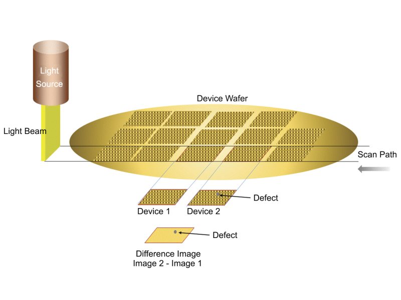
The optical inspection of patterned wafers can employ bright-field illumination, dark-field illumination, or a combination of both for defect detection. Patterned wafer inspection systems compare the image of a test die on the wafer with that of an adjacent die (or of a "golden" die known to be defect free). Image processing software subtracts one image from the other. Any random defect in one of the dies will not zero out in the subtraction process, showing up clearly in the subtracted image (Figure 4). The positions of the defects allow a defect map to be generated over the wafer, similar to the maps generated for non-patterned wafers. As with the inspection of non-patterned wafers, patterned wafer inspection requires precise and repeatable motion control of both the wafer stage and the optical components of the inspection system since they are moved simultaneously.
DUV Wafer Inspection for Sub-100 nm Features
Defect inspection for sub-100 nm patterned wafers presents greater challenges than for non-patterned wafer inspection. DUV-based optical inspection for patterned wafer applications uses the same image comparison principle as older VIS and UV light inspection systems. However, DUV-based methods require a much greater degree of sophistication in the optics, motion control, and image analysis algorithm.
DUV inspection tools have become the industry standard for patterned wafer inspection down to 65 nm feature sizes; inspection rates of up to several wafers per hour make these systems suitable for production applications. DUV inspection tools have demonstrated high sensitivities for the detection of defects such as shallow trench isolation voids, contact etch defects, and photoresist micro bridging at sub-100 nm geometries. Using broadband DUV/UV/VIS illumination, modern bright field patterned wafer inspection systems currently achieve the required sensitivity for defect inspection of all layers on DRAM and flash devices down to 55 nm feature sizes.
While their well-understood characteristics coupled with relatively low cost and high throughput make the continued use of DUV optical inspection systems attractive, some manufacturers have reported that DUV inspection systems do not have the needed precision and sensitivity for geometries below 65 nm. One study claims that the limiting defect sensitivity for DUV dark-field optical pattern inspection systems is about 75 nm in memory technology (e.g. SRAM) and much larger on logic areas. DUV bright-field systems have somewhat better limiting sensitivities, ~50 nm in SRAM and, as with dark-field, larger in logic. Furthermore, the use of DUV lasers to illuminate very small and consequently fragile structures on patterned wafers has produced some unusual problems such as laser ablation of surface material. The solution to these problems may lie in the use of either broadband plasma illumination for optical inspection systems (existing DUV systems employ 266 nm wavelength and are moving to 193 nm illumination) or in the use of production-capable electron beam inspection tools. Recently-introduced inspection tools based on plasma-generated broadband illumination are available for use in production environments. Sub-10 nm resolution is claimed for these systems, because shorter wavelengths provide more accurate inspection at this smaller scale.
E-beam Wafer Inspection
Reticle Inspection
Arguably, reticle inspection is far more important than either non-patterned or patterned wafer inspection. This is due to the fact that, while a single defect on a bare or patterned wafer has the potential to "kill" one device, a single, undetected defect on a reticle can destroy thousands of devices since the defect is replicated on every wafer processed using that reticle. With EUV this problem is further complicated by the finer resolution of the pattern, the presence of a thin protective membrane, and the reflective design of the reticle.
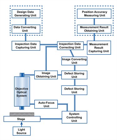
Reticle inspection systems work on the same principles and have similar physical requirements as wafer inspection tools, with the exception that reticles are normally inspected using transmitted rather than reflected light. Transmitted light is used to locate UV-opaque stains and other transmission defects. Reticle inspection tools employ high resolution imaging optics and either VIS or UV illumination, depending on defect tolerances and/or feature sizes, to find defects on a reticle blank or a patterned reticle. Inspections are routinely performed during the reticle manufacturing process and throughout the reticle usage. Reticle inspection tools employ sophisticated image analysis software and motion control systems similar to those used in wafer inspection tools. The use of conventional optics in reticle inspection systems has been extended down to 90 nm feature sizes by using UV illumination. Reticle inspection at smaller feature sizes is possible using EB since lower throughputs can be tolerated in comparison to patterned wafer inspection. As with wafer inspection, the reticle inspection tools used in sub-100 nm applications (both blank and patterned reticle inspection) employ DUV illumination, typically using a single wavelength at 266 nm or 193 nm. Figure 5 shows a block diagram of a reticle inspection platform. Note that, in addition to the objective optical system, motorized stage, and light source, the platform employs various controllers and data analysis modules. Reticle inspection systems can be configured to employ either transmitted light through the reticle or reflected light from the reticle surface in the inspection process. As with other inspection systems, this reticle inspection tool requires highly accurate and precise motion control for the optical components and the air bearing reticle stage.
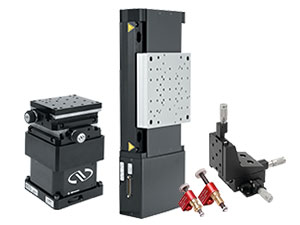
Motion Control for Semiconductor Inspection
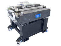
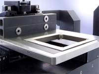
We offer a variety of high performance air bearing stages suitable for use in wafer inspection tools and other motion control applications. The HybrYX™ XY Hybrid Air Bearing XY Stage is a relatively low cost, single plane air bearing stage that is well suited for semiconductor wafer inspection systems and many other scanning applications requiring ultra-low velocity ripple & dynamic following error. The HybrYX stage has a true single place XY architecture with available theta and Z-Tip-Tilt solutions. It features scanning velocities of up to 600 mm/sec and 0.6G acceleration and large (>1 meter) XY Travel range The HybrYX system has a demonstrated and reliable, long-life operation ideal for high duty cycle environments such as wafer inspection applications. The DynamYX® family of reticle positioning stages were specifically designed for semiconductor wafer processing and inspection applications. They offer the highest level of commercially available positioning performance. The extensive use of ceramic materials in these stages provides exceptionally rigid structural stability. They are designed with a low profile that aids in OEM applications.
Custom Optical Solutions for Wafer Inspection
We offer optical sub-system design and manufacturing solutions for wafer inspection tool manufacturers. We have designed and manufactured optical sub-systems for lithography, wafer inspection, excimer and EUV light source, metrology and mask writing applications, among others.
Semiconductor Inspection Products


For additional insights into photonics topics like this, download our free MKS Instruments Handbook: Principles & Applications in Photonics Technologies
Request a Handbook