Solar Panel Manufacturing
The sun provides 1 kW / m2 of free, non-polluting power for several hours every day. Thermal and photovoltaic systems take advantage of this as does the biomass. Coal, oil, plant ethanol, and wood are all forms of stored solar energy. While each energy conversion process has a unique spectral responsivity curve, most laboratory development work has concentrated on photovoltaic (PV) systems. Detailed knowledge of solar irradiance through the VIS and near IR is needed for cell optimization and economic viability assessment.
Photovoltaics
Crystalline-Silicon (c-Si) solar cells are the predominant solar cell technology used in fabricating solar panels because of the availability of silicon, well-developed manufacturing processes, and the high conversion efficiencies that can be achieved. Passivated Emitter Rear Contact (PERC) technology has been shown to generate absolute cell efficiency gains of a percentage point or more compared to conventional cells. In a conventional solar cell, there is an aluminum metallization layer that makes contact across the full area of the back of the cell. PERC technology involves creating a dielectric passivation layer on the rear side of the cell with openings to allow electrical contact to the metallization layer. PERC cells achieve higher efficiencies for a few reasons. First, the passivation layer significantly reduces electron recombination near the back of the cell, where the electrons would otherwise experience a strong attraction to the aluminum metallization layer. This allows more electrons to reach the front-surface emitter, thereby increasing current density in the cell structure. Secondly, the passivation layer enhances the cell's ability to capture light, particularly at longer wavelengths, because it causes multiple reflections, thereby enhancing the probability of absorption. In this way, the absorbing length of the cell is effectively doubled and current density is further improved. Finally, the passivation layer reduces heating of the backside metallization layer by reflecting IR light out of the cell. IR light that is not absorbed by the silicon (. > 1180 nm) would otherwise be absorbed by the aluminum and increase the heat in the cell. Cells are more efficient when operating at a lower temperature.
Solar PV PERC Processing
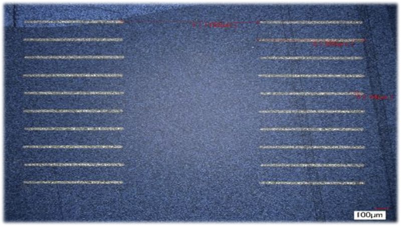
Lasers are used for creating openings in the dielectric passivation layer for ohmic contact. Aluminum paste is screen printed to this surface and a subsequent thermal annealing process alloys the aluminum with the laser-exposed silicon to form a good ohmic contact. A typical 6 inch PERC cell will have about 155 laser-scribed lines which are longer than 156 mm, 40-50 µm wide, and are separated by 1 mm. The aggregate length of the PERC scribes on a single wafer is approximately 25 m. The target processing time can be as fast as one second per wafer, which equates to a 25 m/s required scribing speed. Fast two-axis galvo scanners as well as spinning polygon scanners can achieve such speeds. MKS Spectra-Physics has demonstrated high-quality solar cell scribing for PERC processing as shown in Figure 1.
Industrial PERC processing also requires a laser that can keep up with the high scan speeds demanded. For this, MKS has tested the Spectra-Physics Quasar 532-75 high-power hybrid-fiber laser with TimeShiftª programmable pulse technology. The laser offers both high power and high PRF along with short pulse widths below 5 ns. For thin film removal, shorter pulse durations have been shown to be more energy efficient compared to longer pulse durations. With the Quasar laser, the shortest pulse durations are generated at the highest operating frequencies, which is ideal for PERC processing. Less heating and reduced risk of thermal damage to the underlying c-Si lattice are additional benefits of short-pulse processing. Further throughput improvement is also possible via beam-splitting. When a Quasar laser is operated at 850 kHz PRF, corresponding to one wafer per second (WPS) throughput, the available pulse energy is approximately three times more than necessary. Therefore, a three-beam split can effectively triple the throughput of a single laser thus allowing for throughputs of three WPS. Irrespective of the final system configuration, the Quasar laser platform and its unique TimeShiftª pulse-tailoring technology has the power, speed, and flexibility to meet the demands of industrial PERC solar cell manufacturing.
Tunnel Oxide Passivated Contact (TOPCon) Processing
One technology which shows promise of meeting the growing demands of solar panel quantity, performance and cost-effectiveness is TOPCon, or tunnel oxide passivated contact, technology. Incorporating some laser operations to the TOPCon process can further improve photovoltaic performance.

First, the LDSE process, which stands for "laser-doped selective emitters," creates a shallow, highly doped n++ emitter region by adding an n-type dopant to the wafer and then using a laser to both ablate the anti-reflective coating layer and drive the dopant into the underlying silicon. This would be performed before growing the tunneling silicon oxide layer. The benefits of LDSE include improved overall cell efficiency compared to standard methods such as furnace-based doping.
Solar PV Perovskite Processing
Ever since the first c-Si solar panels were deployed, there has been a continuous quest for higher efficiency and lower cost panels. A second-generation material, cadmium telluride (CdTe), is a thin-film semiconductor that has begun to achieve commercial success. Although not as efficient as silicon, CdTe is lower cost. A third-generation material, Perovskite, could be a game-changer. It has the potential for both higher efficiency and lower cost compared to c-Si and CdTe.
Perovskite can also be used to construct tandem solar cells, which can more efficiently cover a broader absorption spectrum. Another major advantage of Perovskite over silicon is that it is easier to manufacture, as it uses a low-cost ink-based process and does not require high-cost factories and equipment. Moreover, Perovskite can be synthesized from common, recyclable chemicals, of which there is a rather abundant supply. Although Perovskite has not yet reached full commercial viability, the growth rate of its demonstrated efficiency has been faster than that of silicon and CdTe.
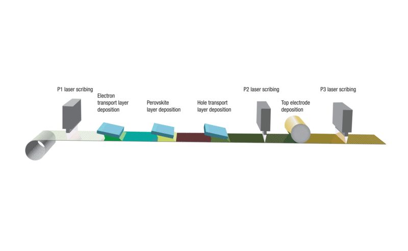
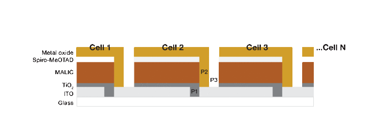
Perovskite solar cell manufacturing is a roll-to-roll process. Part of the process involves removing very narrow portions of thin-film layers of material in a multi-film stack without delamination or debris. This is commonly referred to as "patterning" or "scribing," which is done to achieve monolithic serial interconnections with adjacent cells. Traditional mechanical scribing methods, such as with a blade, and wet chemical etching methods have limitations and may cause undesired problems. By contrast, lasers provide the optimal solution for Perovskite solar cell manufacturing.
Characterization of Photovoltaics
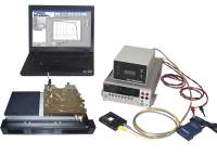
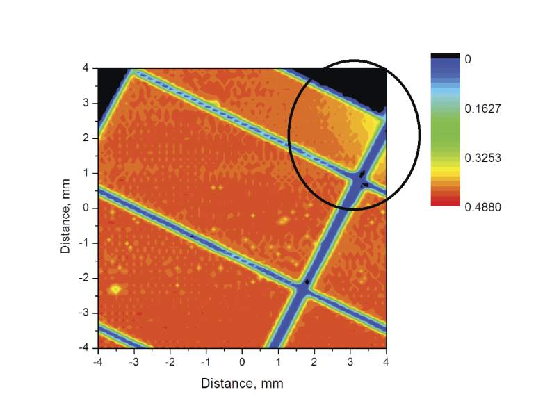
Characterization of photovoltaics involves measurement of current voltage relationships under standard illumination and temperature conditions. Surface reflectance, deep level traps, carrier diffusion, crystalline structure and boundaries, junction type depth and temperature, optical absorption and scattering, series and shunt resistance and photon degradation all influence efficiency. The spectral responsivity curve takes many of these fundamental effects into account, but should record the temperature and intensity level and other measurement conditions for completeness. For example, voltage sweep rates and direction and contact resistivity also affect I-V measurements. Simulator pulse duration is important for some heterojunction and electrochemical cells.
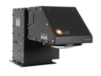
Filtered xenon arc simulators are acknowledged to provide the closest match to standard solar light conditions. Oriel® Solar Simulators were used for some of the earliest development of photovoltaics for spacecraft, and we've improved them continuously.
The high color temperature of the xenon arc is particularly important for devices with blue responsivity. The small bright arc allows the collimation required for test purposes. Our beam homogenizers ensure output beam uniformity over the entire beam area, important for credible testing of any photovoltaic cell. Our power supplies alleviate concerns of output stability; arc wander is minimized. Optional Light Intensity Controllers reduce temporal variations even more.
Solar Panel Manufacturing Products
For additional insights into photonics topics like this, download our free MKS Instruments Handbook: Principles & Applications in Photonics Technologies
Request a Handbook