Optical Transceiver Physics
The devices that transmit and receive data, known as transceivers, are some of the primary enablers of growth in the datacom market. MKS provides optical-to-electrical (OE) converters that are important for the design, manufacture, and testing of optical transceivers. These OEs enable the production line testing of optical transceivers by converting incoming photons into an electrical current that can be measured using conventional production test equipment such as oscilloscopes.
OE converters typically employ photodiodes to absorb incoming photons and convert them into electrical current. Photodiodes are devices in which p-type, n-type, and intrinsic semiconductors are arranged as shown in Figure 1. This structure is known as a p-i-n type diode, where "i" represents the intrinsic undoped layer between the n and p layers. The intrinsic layer absorbs photons and transfers their energy to electrons in the atoms. This transfer of photon energy frees electrons from the atoms and simultaneously generates holes. The electrons migrate to the p-type region where they are collected by the anode (positive terminal) of the device while the holes move towards the n-region and the cathode (negative terminal). In this way, the incoming photons are converted to an electrical current. The mechanisms for photocurrent generation in p-n and p-i-n photodiodes are discussed in Radiometric Measurement and Photoreceiver Characteristics
.
Fundamentals of OE Conversion
.
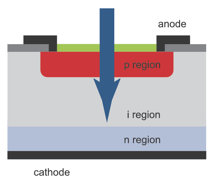
Figure 1. Schematic drawing of p-i-n photodiode(the green layer is an anti-reflection coating).
A major consideration in the selection of photodiodes used in OE applications is the semiconductor material employed. The material determines the wavelength range over which the device will produce usable current and Table 1 shows these ranges for semiconductor materials that make up common photodiodes. Within this range, the semiconductor will generate higher current at certain wavelengths and this is referred to as the device's spectral responsivity. Figure 2 shows a typical responsivity curve for an InGaAs photodiode. The choice of semiconductor material also determines, in part, the dark current of the device which dictates the achievable SNR and detector sensitivity. Since most communication applications employ SWIR laser light, the strong responsivity and low dark current for InGaAs explains why this has become the most popular material for photodiodes used in OE applications.
| Semiconductor Material | Wavelength Range | Dark Current |
|---|---|---|
| Silicon (Si) | 200-1100 nm | Medium |
| Germanium (Ge) | 800-1600 nm | High |
| Gallium Arsenide (GaAs) | 400-900 nm | Low |
| Indium Gallium Arsenide (InGaAs) | 500-1800 nm | Lowest |
Table 1. Wavelength range and dark current capabilities of common photodiode semiconductor materials.
The physical structure of a photodiode has a strong influence on its electrical characteristics. For example, small diameter photodiodes can be advantageous in optical communications applications that require bandwidths exceeding tens of GHz because current rise/fall time is inversely proportional to the device active area diameter (see Photoreceiver Characteristics for details). However, smaller diameters also require that incoming light be directed to a much smaller surface area, e.g., a 30 GHz p-i-n photodiode has an active diameter of only 20 µm. Coupling the light becomes increasingly challenging as network speeds increase since further reduction in the photodiode active areas requires tighter focusing of the optical beam. Furthermore, a laser beam focused to a very small spot size greatly increases the power density at the photodiode surface. This high density can physically damage the photodiode (see Photodiode Sensor Physics) and can cause other undesirable non-linear effects in the device. Consequently, power levels should always be considered as part of communication system design.
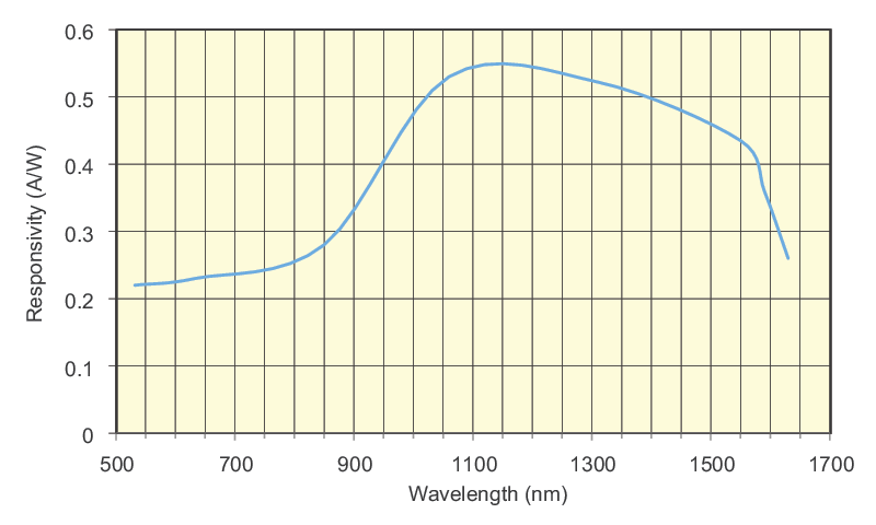
Figure 2. InGaAs Responsivity Curve.
Advanced Photodiode Designs
Figure 3. An optical waveguide.
APDs are also used in data communications networks. A cross-sectional view of an APD is shown in Figure 4. These devices employ an avalanche effect to internally amplify the photocurrent signal. APDs are ideal for low intensity signals and for communication over long distances where attenuation diminishes the signal.
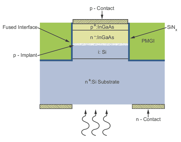
Figure 4. Schematic cross-section of wafer-bonded Si/InGaAs heterojunction APD.
OE Device Design
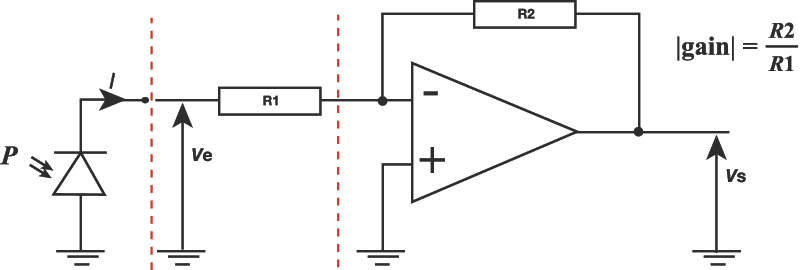
Figure 5. Electrical schematic of typical OE converter.
The effective coupling of photons into fast photodiodes can be extremely challenging. As noted above, a 30 GHz photodiode has an active diameter of only ~20 µm. In communications applications, a typical single-mode optical fiber propagating light at 1550 nm has a 9 µm core diameter and an NA of ~1.4 (see Fiber Optic Physics for more details). This means that the optimal focus distance of the fiber from the photodiode surface is around 80 µm and that there is a tolerance of ± 0.25 µm in both X and Y positioning (see Figure 6). Positioning of the photodiode and fiber for optimal coupling requires automation and the best available motion control products. Positioning becomes even more challenging in applications that require multimode fibers with 50 µm core diameter. In this case, advanced optics are required to focus the beam and these additional optics make the process even more sensitive to misalignments.
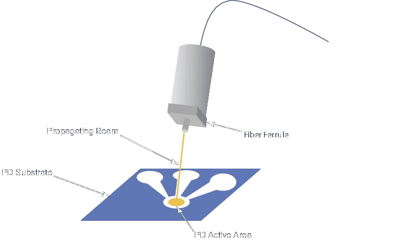
Figure 6. Depiction of the coupling of light from a single-mode fiber to a photodiode (PD) surface.
Application of OEs in Optical Transmitter Testing
Summary of Transceiver Requirements
A summary of transceiver and associated OE converter requirements is given in this section.
- Bandwidth: Currently, the 100 GbE build out requires optical transceivers that can deliver and receive four channels of 25 Gbit/s NRZ data streams. An OE and oscilloscope combination must possess sufficient bandwidth to test each of these channels during the manufacturing process. This means that the frequency response of each component at the -3dB point (the point where there is a 50% loss in signal) must be > 25 GHz. The MKS 1484-A OE meets this specification. Since 400 GbE became standardized with 25 Gbit/s streams still being used, the PAM-4 modulation scheme was implemented since it provides twice as much data per symbol and 8 channels. Nonetheless, there is a desire to return to 4 channels of data streams so that existing infrastructure can continue to be used. However, this will require that the data rate increases from 25 Gbit/s per lane to 50 Gbit/s per lane. The OE and oscilloscope bandwidth needed for such a configuration is therefore > 50 GHz. MKS OEs are meticulously tested and tuned for optimal frequency response performance for any given application. All frequency response and pulse response data are provided for every MKS OE. Wavelength Most 100 GbE data center build outs are driven by the use of a VCSEL operating at 850 nm. InGaAs photodiodes, can also be used for OE conversion at this wavelength owing to their extended responsivities while still being optimal for SWIR applications. Since 400 GbE is being driven at ~1310 nm, InGaAs will continue to be the semiconductor material of choice for these applications. MKS OEs utilize both internal and external p-i-n photodiodes with advanced anti-reflection coatings to help improve responsivity.
- Noise: While the lowest possible noise is generally preferred, the noise requirements depend on the application. Long haul communications require much lower noise specifications than short haul metro or even communications within a data center. Long haul communications typically use dual-matched receivers for coherent detection to help remove background noise from the signal. Short haul metro or data center communications do not require coherent detection, but still require that the NEP be on the order of a few tens of pW/Hz1/2. Low noise requirements mean that it is advantageous for an OE manufacturer to minimize dark current noise in the photodiode and any other sources of electrical noise throughout the circuit. MKS OEs uses proprietary methods to minimize noise. These start with the optical signal and include meticulous calculations and testing of every electrical component.
- Gain: Depending on the application, OE gain requirements may vary from 10 to 1500 V/W. Multiple amplifiers in series can be used to generate more gain. However, a tradeoff exists if the initial signal does not have a low NEP, since amplifiers have bandwidth limitations and are not easily combined at higher bandwidths, i.e., > 15 GHz. Rather, it is best to use a single amplifier that is designed for high bandwidth applications. MKS OEs utilize state-of-the-art amplifiers that have been rigorously tested for quality and reliability.

For additional insights into photonics topics like this, download our free MKS Instruments Handbook: Principles & Applications in Photonics Technologies
Request a Handbook