Semiconductor Lithography
Lithography is defined as "a method of printing from a flat surface (such as a smooth stone or a metal plate) that has been prepared so that the ink will only stick to the design that will be printed". In semiconductor device manufacturing, the stone is the silicon wafer while the ink is the combined effect of the deposition, lithography and etch processes that create the desired feature. Since lithography for device fabrication involves the use of optical exposure to create the pattern, semiconductor lithography is commonly called "photolithography". As with the inspection and metrology techniques already discussed, photolithography is the technique of choice for patterning because it is optical, and thus enables small features and high wafer throughput. This contrasts with other techniques such as direct writing and imprint.
Basic Principles of Photolithography
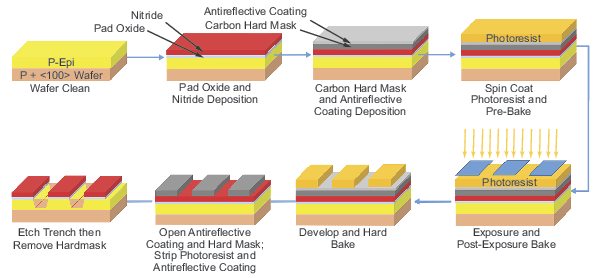
Figure 1 illustrates a typical photolithography process used to define shallow trench isolation features. Such a process consists of the following steps:
- Substrate cleaning and preparation
- Form layers of thermal oxide and deposit a layer of silicon nitride on the clean substrate
- Deposit a carbon hard mask followed by a layer of anti-reflective material
- Deposit a layer of photoresist
- Pre-bake the photoresist
- Align the substrate/photoresist and reticle and expose the photoresist using UV radiation and 4x-5x imaging. Step and scan to repeat
- Post exposure bake
- Develop the pattern in the photoresist and hard bake to remove remaining solvent
- Perform etch to open dielectric anti-reflective coating (DARC) and hard mask pattern and remove photoresist and DARC
- Perform etch to open trenches in substrate and remove hard mask
- Clean surface
Deep UV Photolithography
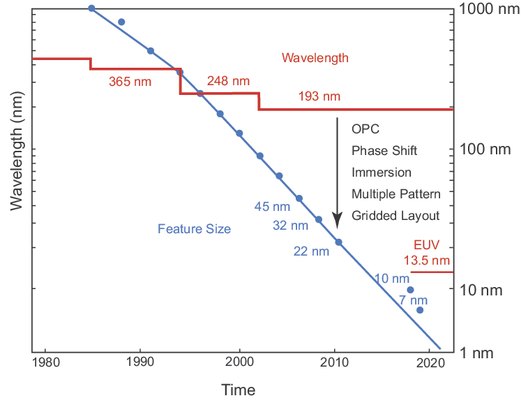
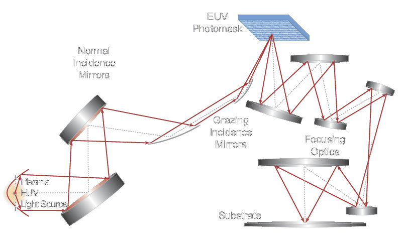
Extreme UV Photolithography
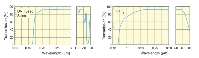
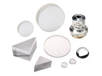
Precision DUV Optics
Optics fabricators have methodologies for eliminating or limiting the effects of photo-molecular contamination that can help achieve high performance, long lifetime optics and systems. These include proprietary optical materials and compounds, proprietary polishing, cleaning and coating processes, and cleanroom handling equipment and processes. This section describes the capabilities that set DUV optics apart from standard catalog optics, including:
- Extensive R&D in materials science
- Reliability and lifetime testing
- Initial design of the system
- System design for long life and minimal preventative maintenance cycles
- Sub-tier supply chain management and control
- Internal cleanroom environments and production control
- Preservation of cleanliness and packaging
Precision Optics for Photolithography
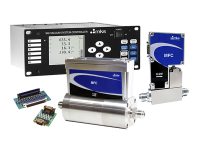
Vacuum Control for EUV Photolithography
EUV places strict requirements on specifications for optical assemblies and vacuum control. EUV light sources require hard vacuum because all gases absorb 13.5 nm light. Process control equipment like MKS flow controllers, valves, and pressure gauges are used.
MicroPirani™/Piezo gauges contain two gauges in one package: a MEMS MicroPirani sensor and a Piezo sensor. They are designed for load locks, measuring pressures that range from atmospheric pressure down to medium vacuum (1000 to 1x10⁻⁵ Torr). This wide range allows the gauge to be used in vacuum chamber applications requiring absolute vacuum/pressure switching capabilities.
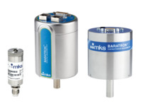
Baratron capacitance manometers provide accurate, repeatable measurements of pressure which are stable over long periods of time. They are an ideal choice for measuring pressure and vacuum in many semiconductor and critical thin film applications, including photolithography for semiconductor device manufacturing and optical coating. Baratron manometers are constructed from corrosion resistant materials and are insensitive to the types of aggressive process gases, such as halogens, typically used in semiconductor etch processes. Baratron manometers for typical semiconductor applications have full scale pressure ranges from 20 mTorr up to 1000 Torr.
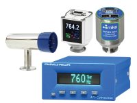
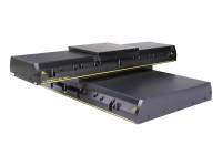
Vacuum Control Products
Accurate Motion Control for DUV Photolithography
In addition to the higher velocities, throughput is also maximized by increasing the die size so that fewer dies are processed per wafer. However, this approach increases the requirements for positioning accuracy. Lithography applications require motion stage calibration to ensure repeatability in the positioning of many different stages in the fab.
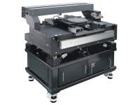
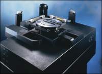
MKS offers a series of high-performance air bearing stage solutions suitable for use in semiconductor photolithography applications and customized tools for automated manufacturing and process control. These extremely rigid structures can accommodate wafers with diameters up to 300 mm. Very high accelerations (up to 5G in some models) and velocities (400 mm/sec to 1000 mm/sec) are achievable while simultaneously retaining high repeatability (25 - 50 nm) and accuracy (0.2 - 0.4 .m). MKS performs high-accuracy calibrations on all stages that achieve operational stability and high positioning accuracy and enable the same level of accuracy from tool to tool.
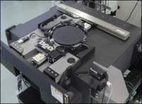
The MKS Z Tip Tilt and theta stage provides high accuracy positioning for large dies and features and an autofocus capability to dynamically maintain the Z position of the wafer, enhancing the throughput of lithography systems. For example, the DynamYX GT stage provides six degrees of freedom for wafer positioning (XYZ, tip, tilt, theta) with XY position accuracy of ± 150 nm over 300 mm. It has flatness of ± 200 µm over this range and step settle for 25 mm (± 50 nm) within 200 ms. The DynamYX DATUM GT stage supports 600 mm panel sizes for panel processing, increasing process throughput in these large-scale applications.
Motion Control Products for Photolithography
For additional insights into photonics topics like this, download our free MKS Instruments Handbook: Principles & Applications in Photonics Technologies
Request a Handbook