Semiconductor Manufacturing
This application note provides a brief overview of semiconductor manufacturing and describe the various optical techniques used to define, inspect, and measure feature sizes and layer properties throughout the manufacturing process. For more information please see Laser Diode and LED Physics.
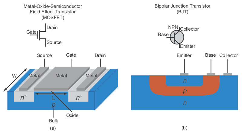
Figure 1. (a) Metal-oxide-semiconductor field effect transistor (MOSFET) symbol and structure;(b) bipolar junction transistor (BJT) symbol and structure.
ICs are composed of layers of materials with different electrical properties, i.e., semiconductors, insulators, and metals. These materials are patterned on a substrate surface in such a way that they form microscopic electronic devices (transistors, resistors, capacitors, etc.) that, when connected by patterned metal lines, produce an IC. Transistors constitute the heart of an IC and their function and design generally fall into one of two categories (see Figure 1): metal-oxide-semiconductor field-effect transistors (MOSFETs) or bipolar junction transistors (BJT). Such transistors are used in many circuit applications, including logic, microprocessors, dynamic random access memory (DRAM), and flash memory (also denoted as NAND). Figure 2 shows a specific example of a CMOS digital IC that illustrates the backend metal connections, and the transistors formed directly on the surface of a silicon substrate. Such CMOS circuits contain complementary and symmetrical pairs of p-type and n-type MOSFETs for logic functions.
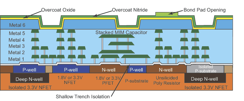
Figure 2. Cross-sectional schematic of CMOS device.
New IC architectures are continually being developed that achieve higher integration densities, functionalities, and performance. Figure 3 shows some examples of the different approaches used to improve cost and function. 3D NAND architectures stack memory cells like a skyscraper to reduce the overall footprint; FinFet logic transistors use a 3D approach to transistor design that reduces electrical leakage; and DRAM is scaled to ever smaller sizes. The rate of increase in functionality and performance has followed the famous Moore's law curve that predicts a halving of cost every two years. However, as device design rules move into the few nm regime, the basic laws of physics have acted to slow the rate of improvement in cost and function, preventing new IC architectures from maintaining Moore's law. However, new heterogenous integration schemes, sometimes referred to as "more than Moore", are being used to continue the scaling.
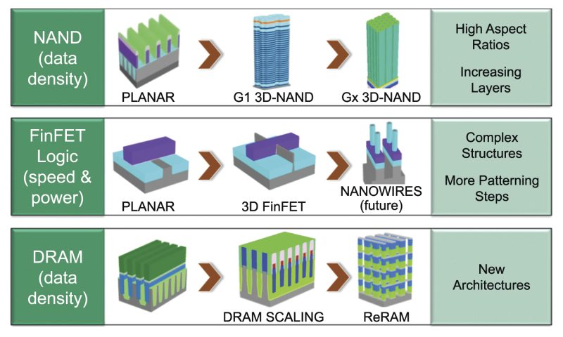
Figure 3. 3D device road map (figure is reprinted with permission of Nanometrics.
Figure 4 shows the relative number of processing steps required for past technology nodes, with 500 needed for the 45 nm node. More recent nodes, such as at 7 nm, require more than 1000 processing steps. The number of processing steps required in a device fabrication scheme can be seen to scale with increasing complexity in the device. More importantly, each additional step adds time and cost to the production of an IC and increases the likelihood for critical defect formation. The need for multiple patterning steps, i.e., litho-etch-litho-etch, to reduce the minimum feature size may be reduced to some extent through the use of advanced EUV lithography (discussed below).
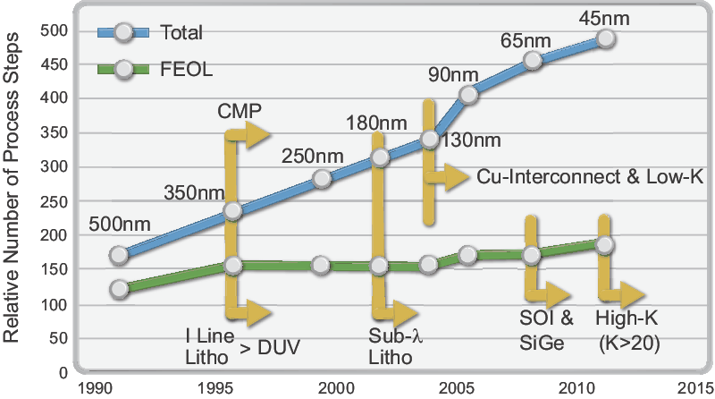
Figure 4. Evolution of process complexity and inflections.
Semiconductor device manufacturing requires hundreds of sequential processing steps to produce a functional, cost-effective device and each step must be performed with near perfection to avoid the creation of a device-killing defect. The MKS Handbook of Semiconductor Devices and Process Technology provides a detailed discussion of device fabrication and therefore this section will provide only a brief outline of the process, identifying those steps where precision photonics enable inspection and metrology. The process steps are illustrated in Figure 5 and the sequence is described in more detail in Table 1.
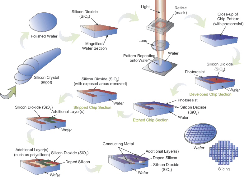
Figure 5. Overview of the semiconductor manufacturing process.
| Step | Title | Description | Inspection (☻)Metrology (Δ) |
|---|---|---|---|
| 1 | Silicon Boule Growth | Electronics grade single crystal silicon boules are grown via the Czochralski process. | |
| 2 | Wafer Fabrication | The boule is ground to the desired diameter, flats are added, and the boule is cut into thin slices (wafers) with a diamond encrusted blade or steel wire. The wafer is ground and lapped to µm-scale surface flatness, while damaged surface layers are etched away. The wafer undergoes chemical mechanical polishing to produce a polished wafer. Epitaxial layers may be deposited. | ☻Δ |
| 3 | Active Area Isolation | Thermal oxidation, nitride deposition, and lithography are used to define the active device areas on the wafer surface. Shallow isolation trenches are etched into the substrate around the active area and filled with deposited silicon dioxide. | |
| 4 | N- and P-Well Formation | The wafer is patterned by coating with photoresist, which is developed selectively using specific wavelengths of intense light shone through a reticle containing the pattern. The light is focused to achieve the final dimensions. N- and P-well regions are formed using ion implantation. | ☻ |
| 5 | Transistor Formation | Thermal oxidation, polysilicon deposition, patterning, and etch are used to produce transistors on the wafer surface. | ☻Δ |
| 6 | Contact Formation | Silicon dioxide deposition, patterning, and etch define contact holes that are then filled with deposited metal. | ☻Δ |
| 7 | First Level Metal Formation | Silicon dioxide or other insulating film is deposited, patterned using lithography and then etched. Interconnects are then patterned in dielectric using lithography and etched. Metal film is then deposited in the openings in the oxide to form the via and metal interconnects. This is called a dual damascene process. Excess material is then planarized using a chemical mechanical polishing step. | ☻Δ |
| 8 | Step 7 is repeated | Step 7 is are repeated to create a multilevel metal structure for back-end connections such as that shown in Figure 2. | ☻Δ |
| 9 | Dicing | The chips are tested and separated for packaging. | ☻Δ |
Table 1. Process sequence in a typical IC device fabrication.

For additional insights into photonics topics like this, download our free MKS Instruments Handbook: Principles & Applications in Photonics Technologies
Request a Handbook