Laser Diode and LED Physics
Semiconductor lasers, generally referred to as laser diodes, are one of the most important classes of lasers today. They are critical for optical communications and control applications and are finding widespread usage as pump sources for solid-state and fiber lasers. Laser diodes possess several unique attributes compared to other types of lasers. They are very small compared to other classes of lasers, can operate very efficiently with relatively low input powers, and are compatible with modern electronics. Many of these characteristics can be attributed to a gain medium that is electrically-pumped while also serving as the resonant cavity. Furthermore, laser diodes leverage mature semiconductor manufacturing processing for good quality control, large-scale production, and tailorability. Laser diodes are a sub-set of solid-state lasers. Therefore, many aspects of the light generation process and output characteristics discussed in the context of solid-state lasers remain valid. However, there are some fundamental differences for laser diodes in terms of the light-matter interactions and the optical emission properties. These differences are addressed in this section. Light-emitting diodes (LEDs), like laser diodes, generate radiation via electrical current injection into a junction. LED light comes from spontaneous emission, whereas laser diode light arises from stimulated emission. Thus, LEDs generally have lower output powers and omnidirectional emission. LEDs are efficient and small like their laser counterparts but typically operate at lower drive currents and are less expensive. Consequently, they have found use in a myriad of everyday applications such as automotive and architectural lighting, remote controls, displays and detection.
The radiating species which make up most laser gain media are either molecules in a dilute gas or liquid, or ions doped in a crystalline or glass host (See Types of Lasers). In a semiconductor, the constituent atoms form a crystalline or amorphous solid that becomes the gain medium. Laser diodes are typically made up of at least two different types of semiconductor materials, and the lasing action occurs at the interface between those two materials. This section gives a brief description of the physics of these interactions and how they enable the generation of radiation.
The atoms making up a semiconductor material have strong interatomic interactions which lead to the formation of valence and conduction bands. These bands are separated by a bandgap energy (Eg) which is analogous to the energy level separation. In semiconductors, an electron that is promoted to the conduction band from the valence band leaves behind an empty state known as a hole. When the electron returns from the conduction band to this empty state in the valence band, a process known as electron-hole recombination occurs. This can result in a radiating photon with a wavelength corresponding to Eg. Clearly, the material and its associated bandgap play a critical role in determining the laser emission wavelength. However, the behavior of an electron in a periodic crystal lattice, i.e., a semiconductor material, requires that both energy conservation and momentum conservation be met during this recombination process. This is most often depicted in a diagram that shows the valence and conduction bands as a function of energy (E) and momentum (k). E-k diagrams for two semiconductors, silicon (Si) and gallium arsenide (GaAs), are shown in Figure 1. When the minima of the conduction and valence bands have the same momentum, as for GaAs, the semiconductor is a direct-gap material. Conversely, Si is an indirect-gap semiconductor where any transition between the bottom of the conduction band and the top of the valence band must include a phonon-assisted change in momentum. A consequence of this is that direct-gap semiconductors emit photons much more efficiently than indirect-gap semiconductors because non-radiative processes tend to dominate in the latter.
Basic Semiconductor Physics
Semiconductor Materials
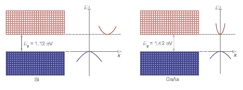
Figure 1. The E-k diagrams for Si, an indirect-bandgap semiconductor, and GaAs, a direct-bandgap semiconductor.
Laser diodes and LEDs almost exclusively use direct-gap semiconductors. Most direct-gap semiconductors are compound materials formed by combining elements from group III in the periodic table (Aluminum (Al), Gallium (Ga), Indium (In)) and group V (Nitrogen (N), Phosphorus (P), Arsenic (As), Antimony (Sb)). These III-V compound semiconductors can be either binary, ternary, or quaternary, depending on the number of elements involved. Changing the compositional mixing ratio of one of the elements creates more material flexibility with the concomitant increase in fabrication complexity. By virtue of this material flexibility, the bandgap energies and associated laser emission wavelengths can span a wide range of the electromagnetic spectrum as shown in Figure 2.
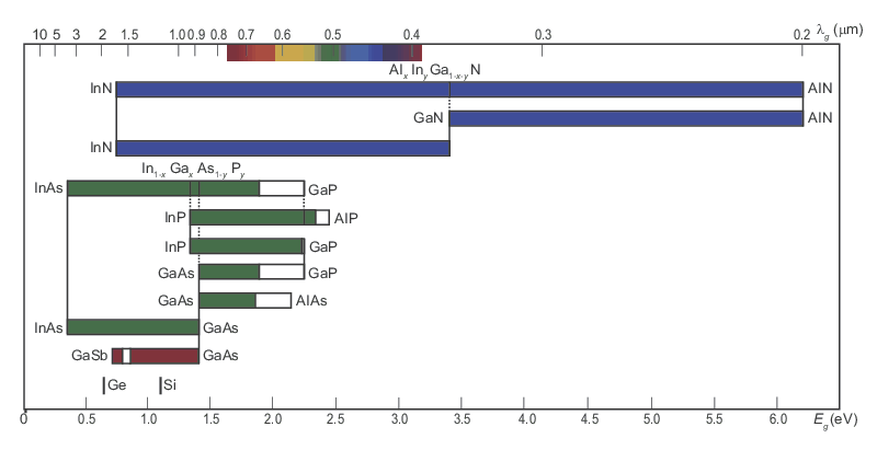
Figure 2. Bandgap wavelength and energy for selected elemental and III-V binary, ternary, and quaternary semiconductor materials. Successive rows, starting at the top, represent AlInGaN, AlGaN, InGaN, InGaAsP, AlInGaP, InGaP, GaAsP, AlGaAs, InGaAs, and GaAsSb. The shaded regions indicate compositions for which the materials are direct bandgap semiconductors.
The semiconductors discussed above are called intrinsic semiconductors. When impurity atoms known as dopants are added to intrinsic semiconductors, the doped materials are referred to as extrinsic semiconductors. The electrical and optical properties of extrinsic semiconductors can be significantly modified depending on the concentration of these dopants. Typically, the dopant atom is similar in size to the intrinsic semiconductor atom but has either one fewer or one greater electron in its valence shell. If the dopants have one greater electron, e.g., a dopant from group VI replacing a group V atom, the resulting material has a surplus of mobile electrons and is referred to as an n-type semiconductor. Conversely, doping with an atom having one fewer electron, e.g., a dopant from group II replacing a group III atom, results in an excess of holes and a p-type semiconductor is formed. n-type and p-type semiconductors are critical in the formation of the p-n junction (see below) which is the essential building block of an LED or laser diode.
The probability of a radiation process occurring is dependent on the population in the participating energy levels (See Light-Matter Interactions in Lasers). Therefore, the efficiency of electron-hole recombination depends on the concentration of carriers (electrons and holes) in the valence and conduction bands. Determining these concentrations requires knowledge of the density of states and their occupation probability, which can be a complicated calculation involving the E-k diagram of the particular semiconductor, the operating temperature, and the doping level. However, qualitatively, the distribution of carriers mimics that of the Boltzmann distribution in that at nominal operating temperatures, the valence band is nearly filled with electrons while the conduction band will be mostly empty. Consequently, in order achieve a significant population of electron-hole pairs for recombination, a pumping mechanism must be present.
Increasing the number of electron-hole pairs in a semiconductor can be achieved through optical pumping as in other solid-state gain media. However, the most convenient pumping method is via electrical injection of charge carriers. This is accomplished by forming a p-n junction diode. When p-type and n-type semiconductor materials are placed in physical contact, the area around the contact (known as the junction) behaves differently than either of the two source materials. The excess electrons and holes diffuse from their respective materials into the adjacent material and recombination occurs. A region on both sides of the junction becomes devoid of free carriers and is known as the depletion region (see Figure 3). An electric field is created across the depletion region by the fixed charges that are left behind following this carrier diffusion. This built-in field, which points from the n-side to the p-side of the junction, prevents further diffusion. This p-n junction is in a state of equilibrium with no current flowing across the diode. However, if an external potential is applied to the junction, the flow of carriers will be affected. If the junction is forward biased such that a positive potential is applied to the p-region, an electric field is produced that opposes the built-in field. Holes from the p-region are injected into the n-region while electrons are injected from the n-region to the p-region. These injected minority carriers recombine with the majority carriers in the destination region (see Figure 3). In effect, radiative recombination is achieved by electrically injecting charge carriers in the junction region. The junction can also be reverse biased, as shown in Figure 3, which is important in the operation of photodiodes.
A homojunction is a p-n junction where both p-type and n-type regions are made of the same material. The first laser diode devices employed homojunctions but were inefficient. This was due to a relatively thick active region (i.e., ~ 1 µm) which is the region of the junction where radiative recombination occurs. The gain coefficient for a laser diode is proportional to the current density injected into the junction. Therefore, reducing the thickness of the active region would allow a smaller volume to be pumped and allow comparable gain with a lower injected current density. Double heterostructure (DH) designs, where the active medium is sandwiched between p and n materials which are different from the active material, allow for reduction of the active region down to thicknesses of 0.1 µm. Threshold current densities can be reduced by nearly two orders of magnitude compared to homojunctions and have largely superseded homojunctions in designs for LEDs and laser diodes. DH devices achieve this thickness reduction by utilizing a narrower bandgap material for the active medium compared to the sandwiched materials. This provides energy barriers at the two junctions and forces injected electrons and holes to occupy a narrow active region. In addition to this carrier confinement, light confinement can also be achieved if the refractive index of the active layer is larger than the cladding layers. The layer acts as an optical waveguide, ensuring that photons are confined to the region where the gain exists.
The probability of a radiation process occurring is dependent on the population in the participating energy levels (See Light-Matter Interactions in Lasers). Therefore, the efficiency of electron-hole recombination depends on the concentration of carriers (electrons and holes) in the valence and conduction bands. Determining these concentrations requires knowledge of the density of states and their occupation probability, which can be a complicated calculation involving the E-k diagram of the particular semiconductor, the operating temperature, and the doping level. However, qualitatively, the distribution of carriers mimics that of the Boltzmann distribution in that at nominal operating temperatures, the valence band is nearly filled with electrons while the conduction band will be mostly empty. Consequently, in order achieve a significant population of electron-hole pairs for recombination, a pumping mechanism must be present.
p-n Junction
A homojunction is a p-n junction where both p-type and n-type regions are made of the same material. The first laser diode devices employed homojunctions but were inefficient. This was due to a relatively thick active region (i.e., ~ 1 µm) which is the region of the junction where radiative recombination occurs. The gain coefficient for a laser diode is proportional to the current density injected into the junction. Therefore, reducing the thickness of the active region would allow a smaller volume to be pumped and allow comparable gain with a lower injected current density. Double heterostructure (DH) designs, where the active medium is sandwiched between p and n materials which are different from the active material, allow for reduction of the active region down to thicknesses of 0.1 µm. Threshold current densities can be reduced by nearly two orders of magnitude compared to homojunctions and have largely superseded homojunctions in designs for LEDs and laser diodes. DH devices achieve this thickness reduction by utilizing a narrower bandgap material for the active medium compared to the sandwiched materials. This provides energy barriers at the two junctions and forces injected electrons and holes to occupy a narrow active region. In addition to this carrier confinement, light confinement can also be achieved if the refractive index of the active layer is larger than the cladding layers. The layer acts as an optical waveguide, ensuring that photons are confined to the region where the gain exists.
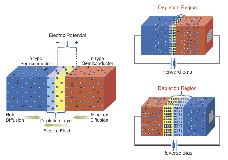
Figure 3. The p-n junction (left) and current flow characteristics of a p-n junction diode (right).
Quantum-Wells DH devices with active layers that are reduced to thicknesses below 10 nm are referred to as quantum-well (QW) devices. By further exploiting the relationship between threshold current density and active layer thickness, QW devices offer excellent performance and are commonly used in laser diodes and LEDs. In conventional DH devices, the active region is large enough that it acts as a bulk material where the conduction band and valence band are continuous. Since the active layer in a QW is smaller than the de Broglie wavelength for a thermalized electron, quantum effects become important. This causes the valence and conduction bands to become step-function bands with discrete energies. In addition to lower threshold currents compared to their bulk DH counterparts, QW devices also benefit from narrower laser linewidths, increased modulation speeds, and a reduced dependence on temperature. There are a variety of device designs utilizing QWs, including multi-QWs, strained-layer QWs, as well as further spatial confinement reduction in the form of quantum wires and quantum dots.
Related Topics
Light-Matter Interactions in Lasers Critical Laser Components Characteristics of Laser Light Methods for Pulsed-Laser Operation Types of Lasers Laser Spectral Tunability Essentials of Laser Safety Optical Emission in Semiconductor Materials Laser Diode and LED Light Characteristics Fundamentals of Laser Diode Control

For additional insights into photonics topics like this, download our free MKS Instruments Handbook: Principles & Applications in Photonics Technologies
Request a Handbook