Insights into High-Speed Detectors and High-Frequency Techniques
Estimating the Minimum Frequency Bandwidth
Knowing your frequency requirement is fairly simple if you are making laser heterodyning or optical modulation experiments. Your equipment should have a fairly flat response out to the highest frequency of interest, usually your highest modulation frequency. Oscilloscopes and other time domain equipment most commonly express their frequency bandwidth in terms of a 3-dB bandwidth (the frequency at which the power falls off to 50% of the value at DC). Amplifiers and spectrum analyzers, however, may express their frequency bandwidth in terms of a 1-dB bandwidth (the frequency at which the power falls off to 80% of the value at DC). In either case, to ensure that the equipment will have adequate bandwidth, determine your highest frequency, add a 20% safety margin, and make this your limiting bandwidth for determining your equipment.
For measuring pulses in the time domain, there really is no definite rule for knowing the required frequency bandwidth. Nonetheless, there is a good way to make an estimate. The photodiode converts photons to electrons. It responds to the intensity of the light; thus, if you relate the FWHM (full-width at half maximum) of the intensity in time to the FWHM of intensity in frequency, you can get some idea of the frequency requirements. For a Gaussian pulse shape with a FWHM of τ, the FWHM in frequency is simply 0.44/τ for a transform-limited pulse; for a sech2, it is 0.31/τ. Using this as your 3-dB bandwidth gives you a very high value, because the 3-dB point specified for electrical devices is where the power, not the voltage, falls to 50% of its value. Equivalently, this is where the voltage drops to √2 of its value. With the photodiode, you are interested in voltage measurements, therefore a more accurate bandwidth is 0.31/τ for the Gaussian or 0.22/τ for sech2. For safety, allow 20% more bandwidth, giving approximately 0.37/τ and 0.26/τ respectively. So on the average, a good rule of thumb is to have a frequency 3-dB bandwidth of 0.4/τ where τ is the FWHM.
Design Considerations for High-Speed Photodetectors
Modeling the photodiode as an RC circuit is commonly known. There are basically three limiting factors to the speed of a photodetector: diffusion of carriers, drift transit time in the depletion region, and capacitance of the depletion region. The slowest of the three processes is the diffusion of carriers to the high-electric field depletion region from outside that region. To minimize this slow effect, carriers should be generated near or in the depletion region. The second process, transit time, is the time required for the carriers to drift across the depletion region and get swept out of the device. With sufficient reverse bias, these carriers will drift at their saturation velocities, on the order of 3x106 cm/s for GaAs. Lastly, the capacitance of the device will determine its RC time constant; R is the load resistance (usually 50 Ω). To maximize a photodiode response, the transit time is typically designed to be comparable to the RC time constant. For instance, given the saturation velocity for GaAs, a 1-ps transit time requires that the depletion layer not be thicker than 0.3 µm. For a comparable RC in a 50-Ω system, the capacitance must be <20 fF, Since C=εA/d (for GaAs ε=13) where the width, d=0.3 µm, and A is the area, your active photodiode area must be a maximum of 52.5 µm2, or a diameter of 8 µm.
Electrical Equipment
Cables
Now that you know the minimum frequency bandwidth that is required to maintain the fidelity of your measurement, and you have chosen a photodiode with adequate bandwidth, every electrical component that follows the photodiode must be able to maintain this bandwidth. Let's first start with your cables. Your typical cable around the laboratory is usually RG-58 which is very lossy after 1–2 GHz. Microwave companies have cables that have acceptable losses up to 50 GHz. These cables have an acceptable loss but it is not negligible. Therefore keep all cable lengths to a minimum!
Connectors
The next thing to keep in mind is that all the connectors must also be up to specifications. This includes the bias T which will allow you to bias the photodetector (note: bias Ts are not necessary with New Focus™ photodetectors). The frequency range of any connector is limited by the occurrence of the first circular waveguide mode in the coaxial structure. Decreasing the diameter of the outer conductor increases the highest usable frequency, while filling the air space with dielectric lowers the highest usable frequency. The BNC (Bayonet Navy) connectors most abundant in the lab are good up to 2 GHz. The SMA (sub-miniature A) connector is good to 24 GHz. The 3.5 mm which uses air as the insulator, can be mated with the SMA and is good up to 34 GHz. The 2.92 mm or Wiltron® K connector1 is good to 40 GHz and is compatible with APC-3.5 and SMA. The 2.4-mm connector is good up to 50 GHz, and the 1.85 mm or the Wiltron V connector is good to 65 GHz. Agilent makes 3.5 mm, 2.92 mm, 2.4 mm and 1.85 mm as well as the SMA, SMC (to 7 GHz), APC-7 (to 18 GHz) and the Type N 50-Ω (to 18 GHz) connectors. The performance of all connectors is affected by the quality of the interface for the mated pair. Great care must be taken with these connectors. A torque wrench which is permanently set to the correct torque value should be used to turn the male coupling nut while grasping the body of the connector firmly to keep it from rotating. As the male coupling nut becomes tighter, frictional forces will increase, and the nut and body will tend to lock up, which will cause the body to rotate. This wears away the plating and can score both the outer interface rim and the pin of both connectors. Once a connector has been over-torqued and damaged, it will damage to some extent each connector to which it is mated. This damage lowers its frequency performance. In addition, never hold a male connector coupling nut stationary while screwing the female counterpart into it. This destroys both connectors.
Instruments (Amplifiers, Oscilloscopes, etc.)
For your electrical instruments, Agilent and Tektronix1 manufacture digital oscilloscopes to 50 GHz and spectrum analyzers to 325 GHz. New Focus™ and other companies have amplifiers to 20 GHz. Remember that the fidelity of your measurement requires that the instrument's response be fairly flat over the frequency bandwidth of interest. This means that both the amplitude response must be flat and the phase response must be linear with frequency. If this is not true of your instrument, for example if your amplifier has a non-linear phase response, then it will distort your measurement. Your measured signal waveform will become slower.
Summary of Electrical Equipment
Let's now look at three different frequency regimes, <1 GHz, DC to 25 GHz, and DC to 60 GHz. If the maximum frequency of interest is <1 GHz, or the pulse width is >400 ps, APDs may be adequate, and BNC connectors and RG-58 cables certainly are. For 0-25 GHz or pulse widths >16 ps, PINs or Schottky photodiodes are required as well as SMA connectors and high-performance flexible or semi-rigid cables. For the bias T, Agilent makes one good to 26.5 GHz as well as amplifiers good to 26.5 GHz. Agilent makes a scope good to 34 GHz, and their spectrum analyzers go to 22 GHz or 26.5 GHz. Tektronix also makes a digital oscilloscope good to 20 GHz, and spectrum analyzers good to 33 GHz. For 0-60 GHz or pulse width > 6.7 ps, you must use the highest quality equipment. This includes 1.85-mm or V connectors, ultralow-loss cables, and the best oscilloscopes from Agilent and Tektronix which both only go to 50 GHz. Wiltron has a bias T for 60-GHz operation. In order to extend to this frequency, the spectrum analyzers must use external mixers. Both Agilent and Tektronix have this capability.
Making a Measurement
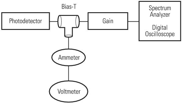
You are now ready to set up your measurement system. Most setups resemble Figure 1. First, bias up the photodiode and measure the leakage current. This should not be very large, hopefully only a few µA. Then apply the optical signal. Since the photodetector active area is probably on the order of 10 µm, focus well. Remember that to achieve the best performance all the generated carriers must be in the depletion region. If they are not in this high-field region, then they must diffuse to the depletion region resulting in a slow long tail on your measurement. In communication systems, this can cause higher bit error rates if the tail interferes with the next bit of information. The best way to focus onto the photodetector is to monitor the photocurrent on the ammeter (resolution on the order of 1 µA) and to observe your signal on the spectrum analyzer which is much more sensitive than the digital oscilloscope. If you are observing pulses from a mode-locked laser source, you should observe the signal at the repetition rate of your laser. New Focus™ detectors simplify this process by providing an amplified bias monitor and built-in bias network. Finally, observe your signal on the digital oscilloscope. The best way to trigger the scope is to use a power splitter to split off some of the signal to the trigger. If there is not enough voltage available, then try triggering off a synthesizer at the same frequency as your laser or signal of interest. However, if you do this you will have to consider that there is timing jitter between your signal and the synthesizer. This will broaden your signal, decreasing its bandwidth. To decrease the amount of timing jitter, trigger off a source that has been phase-locked to whatever is driving your waveform, whether it is your modelocker or another synthesizer.
Actual Pulse Width Measurement
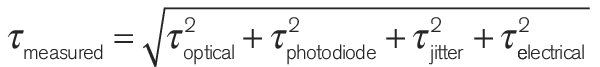
The actual pulse width that you will measure will be a convolution of the optical pulse width, the photodetector impulse response width, all your electrical equipment impulse response widths, and any timing jitter noise. The impulse response width is the width of the output response resulting from an impulse-like (δ-function-like) input. A simple way to estimate the contributions is by using a sum-of-squares technique where the measured pulse width is given by
τoptical is the optical pulse width; τphotodiode is the impulse response of the photodiode (approximately, 0.4/f3-dB); τjitter is the timing jitter, including pulse-to-pulse laser timing fluctuations, synthesizer jitter, etc.; τelectrical is the impulse response of your electrical equipment. Remember each component contributes by the sum of squares. If your optical signal and your photodiode impulse response are the same, and your jitter and electrical equipment impulse responses are much smaller, your measured signal will be approximately √2 larger than the actual optical signal.
Minimum Signal and Noise
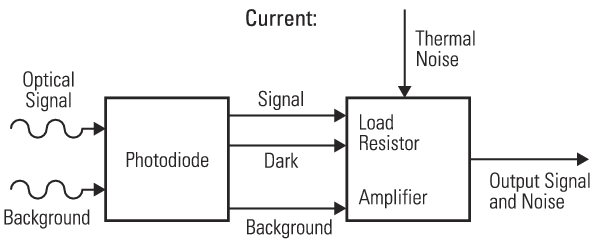
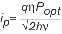
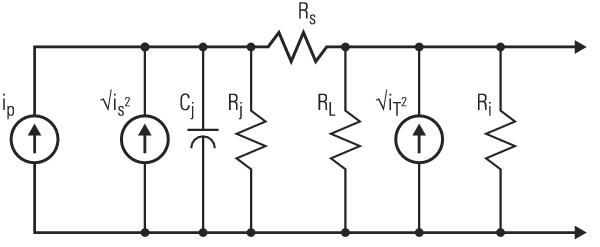
Figure 2 is a simple block diagram of your photodiode and circuitry (for a good reference see Physics of Semiconductor Devices, 2nd edition, S.M. Sze2). The optical signal and background radiation impinge on the photodiode inducing a current in the external load resistor. If P is your average optical power then Ip, the average photocurrent, is given by,
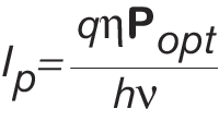
where q is the electron charge, h is the quantum efficiency, and n is the optical frequency of your light. (R=ηλ/1.24, where R is the responsivity, the ratio of photocurrent to the optical power. To convert this to Volts/Watts, simply multiply by the load resistor). For a 100% sinusoidal modulated signal, the rms optical power is given by Popt/√2, and the rms photocurrent, ip, is
Shot noise is noise that is not frequency dependent; it is white noise. In the photodiode case, this random noise, is, is caused by current from the background radiation, Ib and that from the dark current, Id. The dark current is due to thermal generation of electron-hole pairs in the depletion region. The photodiode also has a shot noise from the photocurrent. The total shot noise, that is the meansquared current, is then
<i2s> = 2q(Ip + Ib + Id) B
where B is the bandwidth of your measurement.
The equivalent circuit of the photodiode is shown in Figure 3. The components ip, √2s, Cj, Rj, and Rs are the RMS photocurrent, the shot noise current, the junction capacitance, the junction resistance, and the series resistance. RL is the external load resistor and Ri is the input resistance of the following amplifier. For the reverse-biased Schottky diode, Rj is very large (>106 Ω) and can be neglected next to RL which is typically 50–500 Ω. The series-connected Rs is usually much smaller than the other resistances and can be neglected as well. The thermal Johnson noise is then given by
<i2T>=4kT(1/RL)B+<ii2>
Since the amplifier input resistance may or may not be due to an actual resistor, the noise current due to Ri is listed separately as ii.
With the above information, we can then find the power signal-to-noise ratio which can be expressed as
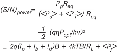
where 1/Req= (1/RL) + (1/Ri).
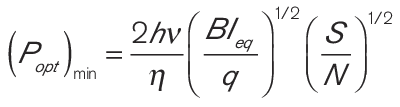
Thus to achieve a certain signal-to-noise ratio, the minimum optical power required is.
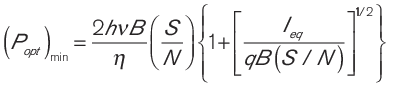
where Ieq= Ib + Id + 2kT/qReq +
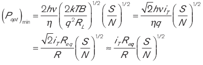
Let's now look at two limits, one where Ieq/qB(S/N) is much less than unity, and the other where this is much larger than unity. If Ieq/qB(S/N) is much less than unity, the dark current, background current and thermal Johnson noise are very small. In this case the minimum optical power is determined by the quantum noise associated with the optical signal. However, this case is very difficult to achieve; in our above example, B(S/N). must be much greater than 6.25 x 10¹⁵ Hz. In the other limit, the background radiation and/or thermal noise of the equivalent resistor dominates. Then the minimum optical power is
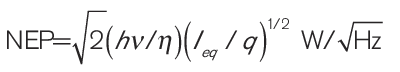
To increase the sensitivity of the photodiode, one would want to increase the quantum efficiency, or increase the equivalent resistor. The noise-equivalent-power, or the optical power required to have S/N=1 (the optical signal is exactly equal to the output noise) over a 1-Hz bandwidth is simply
Now to consider the New Focus™ 1000 Series photodiodes, let <
With the photodiode connected to a 50-Ω system (Ri =50 Ω), Req=33 Ω for the 1001 and 1004, and 25 Ω for the others. Calculating the minimum optical power (λ=0.532 µm) for a S/N=1 and a bandwidth of 1 Hz, you will find that for the 1001 and 1004, the minimum optical power is 60 pW. For the 101X Series, at 1.3 µm, the minimum optical power is 41 pW. A 1-Hz bandwidth implies an integration time of roughly 1s. This is the minimum detectable optical power if all the following equipment were to add no noise. In reality, your electrical equipment will most likely have much worse noise performance; it will not be able to detect 3 nV. Then the worst component will determine your minimum detectable signal. For example, if your oscilloscope is the culprit, the minimum detectable signal will be dominated by its minimum sensitivity of about 1 mV.
Frequency Response Considerations
Finally, let's discuss how various frequency responses will affect your time domain results. Optimally, you would like a flat response out to your frequency of interest. New Focus photodiodes have been individually measured from DC to 45 GHz, and they have a fairly flat response to 45 GHz. Beyond 45 GHz, the responsivity of the diode drops sharply. This is due to the RC pole from the diode in conjunction with other poles from parasitics.
On the other side of the spectrum, it is also important to have a flat response to DC. If there is no response at DC, you are essentially AC coupled and will not be able to measure any DC level. There will be no way to ensure that your modulation depth is complete, and long pulses will be severely distorted. If, on the other hand, the response is peaked at DC, there will be artificially long tails on pulse measurements in the time domain. One possible cause may be that the photodiode is limited by the diffusion effect, possibly from poor focusing. The carriers have been generated outside the active area of your diode. If however, you find that your frequency response is peaked at DC as in Figure 4, and this is not due to a focusing problem, there is an easy way to estimate how this affects your measurement.

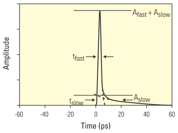
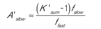
Remember that the Fourier transform of your waveform from the time domain to the frequency domain will result in your frequency response. Moreover, since Fourier analysis is completely linear, you can model a waveform as the sum of fast and slow components. For example, the pulse shown in Figure 5 has an artificially long tail. It can be modeled as the sum of a fast pulse and a slow pulse. Let's say that tfast and Afast are the FWHM and amplitude of the fast component, and tslow and Aslow for the slow component. If your curve resembles Figure 4, first find the 3-dB point of the slow, the lower frequency, and then the 3-dB point of the fast, the higher frequency. From these, you should be able to find tslow and tfast since they are related by t=0.4/f. Then we know that the DC or 0 frequency response is the area under your curve in time. For example, for a Gaussian, the amplitude at DC is related to the pulse width and amplitude in the time domain. The wider the pulse width or the greater the amplitude, the higher the DC response. Thus, K1 is proportional to tslow Aslow while K2 is proportional to tfast Afast. In Figure 4, Ksum=K1+K2. Now, normalize both in the time and frequency domain to the fast pulse. So now, A'slow is that normalized to A'fast, and K'sum is that normalized to K2. This implies that K'Sum≈1 + A'slow tslow /tfast=1+A'slow ffast /fslow. Therefore, once you know the amplitudes, and FWHM, simply sum the two components to get some idea of what your waveform will look like in the time domain.
Lastly, the measured frequency response will give you a good relative measurement from DC to 45 GHz. However, if you wish to make an accurate absolute measurement it is very difficult. This is because you must consider the responses of all your cables, connectors, and equipment. If just one of those is not correct, you will have an error in your measurement. It is necessary to do what New Focus™ has done with its photodiode and measure the frequency response of each and every component. This can be done quite easily with the aid of an automatic network analyzer but is quite tedious without it.
Summary
High-speed optical measurements not only require the generation of fast optical signals, but also the detection of them. In choosing your photodiode and all your electrical equipment, including cables and connectors, keep in mind the frequency response required to maintain fidelity of your signal. Remember that your measurement will be as slow as the slowest component of your system!
References
- For technical assistance, suggestions for equipment selection, and additional references, contact New Focus.
- Sze, S.M., Physics of Semiconductor Devices, 2nd ed., John Wiley and Sons, New York, 1981.