Extreme UV Photolithography
EUV lithography is being developed to fulfill single-exposure patterning requirements at feature sizes below 22 nm (Figure 1). Unique to this technology is the nature of the light source. There is no readily available conventional light source having a wavelength below 157 nm which is the wavelength of light from a F2 excimer laser. The F2 excimer laser source has not gained broad use for lithography at small feature sizes. This is probably due to factors including difficulties with the required CaF2 optics, e.g. increased mask registration errors due to birefringence, and the success of the extension of 193 nm patterning technology that allowed it to function down to the single-exposure limit of 157 nm lithography, i.e., 32 nm. Instead, lithography equipment developers have turned to an entirely new way of generating light at EUV wavelengths for use in lithography at sub-32 nm feature sizes.
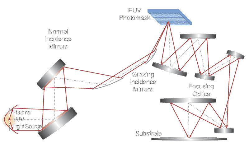
Figure 1. EUV lithography schematic.
13.5 nm light sources of consist of a high-power CO2 laser, laser beam transport and focusing optics, and a light source vessel. Within this system, 13.5 nm light is generated using laser pulsed plasma excitation of tin molecules by a CO2 laser. The light is generated inside a vacuum vessel where droplets of tin pass through the focal point of pulses of high intensity light from the CO2 laser. As the small (~30 µm diameter) droplets of molten tin encounter the pulse of high intensity laser light, they are vaporized, and the tin atoms undergo electronic excitation and ionization, creating a hot plasma with electron temperatures of 10's of electron volts (1 eV = 11,605 K). Electron-ion recombination and ion deexcitation within the plasma emit photons at 13.5 nm. Conversion efficiencies (CEs) for this mode of light generation are relatively low, with CEs of 3-5% reported for some tin-based EUV sources. The light emitted by the plasma is collected using an ellipsoidal collector that reflects it to an intermediate focus at the front of the light source. The mirror is unique in that it is not a conventional polished optical mirror, but rather a Bragg reflector made up of thin layers of molybdenum (Mo) and silicon (Si) designed to reflect the greatest amount of 13.5 nm light. From the intermediate focus, the light is transported to the optical train in the photolithography system using solely reflective optical components. The entire optical system is maintained under high vacuum since 13.5 nm light is strongly absorbed by all solids, liquids, and gases. The mirrors are also Bragg reflectors and can reflect up to 70% of the incident light. They are critical system components that must have extremely low surface roughness (a few atoms) and highly precise flatness and curvature. Since reflection is not 100%, the number of reflectors between the source and the substrate has a significant impact on the energy of the EUV beam at the substrate surface. Since the optics are all reflective, the masks used in EUV scanners must also be reflective, since no optical materials are transparent to EUV. In theory, transmission masks could be used if the substrate was less than 100 nm thick, but this is not a practical solution. EUV masks are fabricated on very low thermal expansion substrates using multilayer Bragg reflector technology. The multilayer reflector has 40-50 pairs of Mo and Si thin film layers each and a total thickness of about 300 nm topped by a capping layer of about 11 nm of Si. A buffer layer, typically SiO2, is deposited on top of the stack, followed by an absorber material with a thickness of about 100 nm. This absorber layer and the buffer layer are patterned to produce the reflective mask.
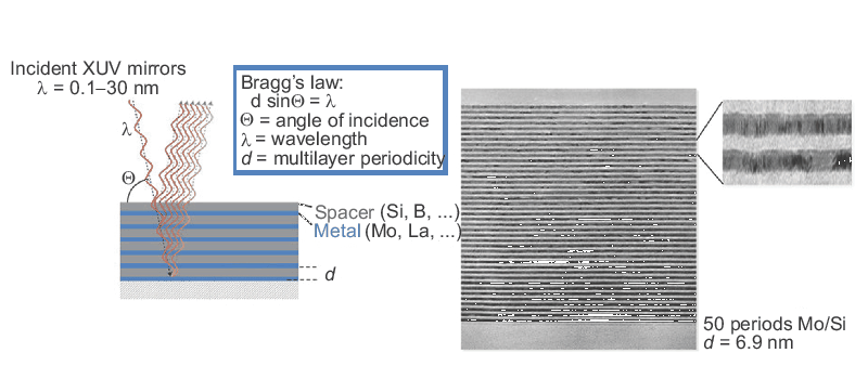
Figure 2. The principle employed in a Bragg reflector (left); cross-sectional transmission electron microscopy image of multilayer EUV mirror grown by e-beam evaporation and ion beam sputter deposition (right). Figure reprinted with permission from F. Bijkerk, University of Twente.
Figure 2 shows a transmission electron microscopy image of the multilayer stack in a EUV mask while Figure 3 provides a simplified process flow for EUV mask fabrication. Since there are no optical materials that are transparent at 13.5 nm, any pellicles employed with EUV masks must be extremely thin (pellicles are the enclosures used to protect the photomask). 50 nm thick pellicle membranes supplied by ASML can transmit 85% of the EUV light (useful for lower power EUV). Great care is required in maintaining these masks in a defect-free state. Transport of masks to and from a lithography tool is performed using specialized dual pod containers to ensure mask integrity. There are currently no actinic inspection techniques for EUV masks, i.e., inspection using a wavelength of light that is similar to the feature sizes on the mask.
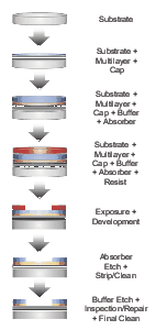
Figure 3. EUV mask fabrication step.
Photoresist materials for EUV continue to be developed and improved. It is expected that photoresist formulations will have some unique requirements compared with conventional resist technology. Chemically amplified resists that served the industry well since the introduction of 248 nm exposure wavelengths appear to have certain inherent resolution/sensitivity trade-offs that will force the development of more advanced resist formulations for EUV technology. Currently, hybrid approaches such as those that employ a sacrificial spin-on carbon film and a resist layer containing organometallic molecular linkages are receiving considerable attention.

For additional insights into photonics topics like this, download our free MKS Instruments Handbook: Principles & Applications in Photonics Technologies
Request a Handbook